
Design, calculation and simulation of planar transformers
Loss physics, winding structures, parasitics, insulation standards and the open-source software ecosystem for high-frequency magnetics.

Executive summary
The drive for higher power density, efficiencies above 98 % and ultra-thin profiles has pushed the transition from the conventional wire-wound transformer to the planar transformer: photolithographically etched copper traces on multilayer PCB or foils, coupled to low-profile ferrite cores. The change is not just form factor; it redefines high-frequency electromagnetic losses, parasitic dynamics and the validation methodology.
This article systematizes advanced planar-transformer design: the loss physics (skin effect, proximity and the Dowell model), turns-number optimization, the interleaved winding structures that control the magnetomotive force, leakage-inductance and inter-winding-capacitance management, experimental and finite-element validation, insulation-standard compliance, and the software ecosystem —with particular attention to the open-source tools that enable first-class engineering without proprietary licences, consistent with Premium SA’s preference for open, auditable software.
All figures and tools are traced: to peer-reviewed technical literature (application notes, DTU/Ouyang papers, IPC/IEC standards) and to verified open-source repositories. The formulas are the classic ones of the domain.
Planar versus conventional: what changes
Conventional round-wire, Litz or foil transformers on PQ/ETD bobbins have severe limitations above 100 kHz, and winding variability introduces parasitic spread that hampers industrial repeatability. The planar replaces coils with copper traces on multilayer PCB or foils coupled to low-profile EQ/ER/E-LP cores. The most visible consequence is geometric; the most valuable, repeatability.
Table 1 — Conventional versus optimized planar transformer (traced to literature).
| Parameter | Conventional (PQ32/35) | Planar (EQ38/8/25) | Engineering implication |
|---|---|---|---|
| Profile height | 30–40 mm | ≈ 10.7 mm (≈ ⅓) | Integration into very low-profile boards (brick) |
| Weight | High | ≈ 3× lighter | Critical in transport and aerospace |
| Parasitic repeatability | Low (high spread) | Very high (photolithography) | Enables precise tuning of LLC tanks |
| HF conduction losses | High (inefficient packing) | Low if Rac is optimized | Better dissipation and overall efficiency |
| Prototyping flexibility | Very high (rewind by hand) | Low (any change = new PCB) | Forces simulation before fabrication |
That last row sets the method: since any minor change requires a new PCB, planar design does not allow bench trial-and-error. It demands rigorous analytical modelling and simulation before going to production.
Systematic design methodology
The move to planar is not the geometric replica of a wire transformer: it requires a structured flow that audits the electrical, thermal and mechanical specifications and adapts them to PCB physics.
Table 2 — Planar design workflow (eight stages).
| Stage | Key action | Critical parameter |
|---|---|---|
| 1 · Base-design audit | Collect V, P, f, Lm, Llk, insulation, temperatures | Thermal and electrical targets to replicate/improve |
| 2 · Core and material | Planar geometry (EQ/ER/E-LP) and ferrite (N87/N95/3C95/3F3) | Balance hysteresis loss vs available height |
| 3 · Number of turns | Np, Ns from Faraday’s law and ΔB max | Fewer turns → less copper but more core |
| 4 · Copper thickness | Size h according to skin depth δ | Avoid oversizing (aggravates proximity) |
| 5 · Stack-up | P/S/shield sequence and interleaving | Determines Llk, Rac and global losses |
| 6 · Trace width | Carry the DC and AC current density | Keep ΔT within safety limits |
| 7 · Electrical/thermal validation | FEA or advanced analytics of HF losses and T | Spot hotspots before fabrication |
| 8 · PCB fabrication | Vias, insulation slots, export Gerber | Manufacturability and insulation compliance |
Loss physics: skin, proximity and Dowell
Accurate conduction-loss calculation is the greatest challenge in HF magnetics. Two coupled phenomena govern it. The skin effect concentrates current in a surface layer of depth δ = √(ρ/(π·μ·f)); for copper at 70 °C it reduces to the practical rule δ ≈ 2.276/√f mm. The resistance increase from this effect is Rac/Rdc = ξ·[sinh(2ξ)+sin(2ξ)]/[cosh(2ξ)−cos(2ξ)], with ξ = h/δ the normalized thickness: when ξ > 2, the conductor centre barely conducts and thickening the copper stops helping.
The proximity effect is more damaging. When layers are stacked, the fields of neighbouring conductors induce cross eddy currents. Dowell’s model for the m-th layer adds a second term scaling with (m²−1), where m is the layer’s MMF factor. Because that term grows quadratically with layer position, losses in stacks with many continuous non-interleaved layers explode. And since real currents are PWM, not sinusoidal, the resistance must be evaluated over the harmonic spectrum —P_AC = Σ Rac(n·fs)·I²rms(n)—: high-order harmonics, with very small δ, dissipate a lot even at moderate amplitude.
The optimal number of turns. Increasing N lowers the flux density ΔB and, via Steinmetz (Pv = K·f^α·ΔB^β, with β≈2–3), reduces core losses; but it demands narrower traces or more layers, raising Rdc and, through Dowell’s m, Rac. The optimum is not to eliminate one term but to balance them: the absolute loss minimum occurs when the copper losses are held at a factor β_loss = P_copper/P_core of the ferrite losses. It is the designer’s analytical tuning criterion.
Winding structures: interleaving as the lever
The way to tame proximity losses is to alter the spatial field distribution in the core window, abandoning simple non-interleaved stacks. Interleaving alternates primary and secondary layers with opposite current directions in adjacent layers, cancelling the net field and reducing Dowell’s m. The figure below compares three stack-ups and their MMF profile.
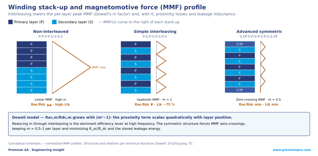
The advanced symmetric structure 0.5P-S-P-S-P-S-P-S-0.5P —with the outer layers at half-turn and connected in parallel— forces multiple MMF zero-crossings, keeping m≈0.5–1 uniformly and minimizing both Rac/Rdc and the stored leakage energy. For fractional ratios or extreme thermal performance in the MHz range, the half-turn structure implements 180° traces in parallel on the outer layers, splitting the current and halving the peak field. And at high current, the interleaved serpentine winding snakes across several legs, maximizing window use without extra interconnection layers.
Table 3 — Winding structures and their behaviour (traced to literature).
| Structure | MMF profile | Rac/Rdc | Leakage Llk | Routing / vias |
|---|---|---|---|---|
| Non-interleaved (P-P-P-P-S-S-S-S) | Linear ramp; peak at interface | Very high (accumulates m) | Very high | Minimal (no crossings) |
| Simple interleaving (P-S-P-S…) | Sawtooth; moderate peaks | Low (m≈1) | Reduced up to −75 % | High (alternating layers) |
| Advanced symmetric (0.5P-S…0.5P) | Attenuated; cancellation at outer faces | Absolute minimum (series-parallel) | Very low and controlled | Very high (parallel vias, symmetry) |
| Half-turn | Shifted and symmetric to axis | Very low (m≈0.5) | Minimal for a given insulation | Very high (fractional geometry) |
Parasitics as design variables: leakage, capacitance and EMI
The planar’s tight spatial coupling maximizes mutual inductance but demands treating parasitics as active variables. Leakage inductance Llk arises from flux that closes through the window without linking both windings. In hard switching (full bridge, flyback) it is a harmful parasitic that causes overvoltages and demands snubbers; it is minimized with full interleaving and thin dielectrics. But in LLC resonant converters it is exploited: a controlled Llk is deliberately designed to act as the series resonant inductor Lr, removing a discrete component and gaining density. To tune it, magnetic shunts are inserted or the inter-layer dielectric spacing (Δh) is adjusted, which raises Llk linearly.
The high-frequency design dilemma. Reducing leakage forces primary and secondary close together, which raises the inter-winding capacitance C_inter. Under the primary’s fast dv/dt, C_inter injects common-mode displacement currents into the secondary, generating conducted EMI that demands bulky filters. It is broken with electrostatic shielding (a thin, slotted copper layer —to avoid shorting the flux— tied to a quiet ground) or with an auxiliary cancellation winding of opposite polarity (−dv/dt) that nulls the net common-mode current.
Validation: leakage measurement and hybrid analytical-FEA calibration
In a high-performance planar, Llk is under 1 % of the magnetizing inductance (often 0.1–0.2 %, in nanohenries), of the same order as the instrument leads’ own inductance. It is measured with the direct short-circuit method (a wide copper bar across the secondary + impedance analyzer at the decade of the switching frequency) or, without an HF analyzer, with the turns-ratio and AC-deviation method. In both cases it pays to build test fixtures with planar contacts and symmetrical coaxial traces to calibrate open/short at the device plane.
The one-dimensional Dowell model fails on real traces: concentric spirals concentrate the DC current at the inner radius (spirality effect), raising the real Rdc. The hybrid analytical-numerical methodology solves this without the cost of a full 3D transient: the ideal arc is computed (Rca = 2π/(σ·h_cu·ln(r₂/r₁))), the real resistance is extracted by static DC FEA with quarter symmetry, a calibration factor (Rca/R₊) is obtained and injected as a coefficient into the AC-loss formula. The result agrees with 3D transient simulations (Ansys Maxwell) within under 1 % error, in microseconds instead of hours.
Insulation and standards: clearance, creepage and IEC 60664-1
The proximity of high- and low-voltage traces demands strict compliance with dielectric standards. Clearance is the through-air distance (prevents direct arcing); creepage, the leakage path along the solid surface (prevents conductive carbonization). IPC-2221 sets minimums up to 500 V and adds a linear surcharge above that; IPC-9592, specific to power conversion, imposes more conservative criteria. High-CTI materials tolerate smaller creepages.
Distances are not read from a static table: IEC 60664-1 requires evaluating the real environment. The pollution degree (PD2 common in industry) can be reclassified to PD1 with conformal coating or potting, drastically reducing the required creepage. The overvoltage category (OVC) sets the primary clearance on mains. And altitude penalizes: above 2000 m the lower dielectric strength of air forces multiplying the clearance, with a factor of about 1.48 at 5000 m —relevant in mountain railway, high-altitude solar and avionics. Physically, creepage is multiplied by milling through slots in the FR4 between primary and secondary, forcing the leakage path to go around the cut, or by interposing insulating barriers.
Software ecosystem: open and commercial
The coupled complexity of the HF field has produced a mature software ecosystem. Premium SA prioritizes, where they meet requirements, open-source and auditable tools: they enable first-class engineering with no lock-in or licence cost, and their verifiable code fits the traceability that regulated sectors demand.
On the open side, the OpenMagnetics project stands out —a working group of the PSMA magnetics committee—: its MKF compute engine (C++) is exposed in Python via PyOpenMagnetics/PyMKF and operates on the neutral MAS format (Magnetic Agnostic Structure, a JSON schema describing requirements, construction and results, with insulation coordination per IEC 62368-1/61558). python-planar-magnetics (on PyPI) generates planar spirals respecting DRC rules, estimates Rdc correcting for spirality, and exports to KiCad (S-expressions) and DXF. For full FEA, ONELAB integrates Gmsh (meshing), GetDP (eddy-current fields coupled to SPICE) and Elmer (3D multiphysics in parallel, couplable to OpenFOAM for conjugate thermal). The Ansyas bridge (Synopsys–Würth collaboration) connects MAS to Ansys Maxwell via PyAEDT.
Table 4 — Software for planar magnetics design (verified).
| Suite | Licence | Base / environment | Capability for planars |
|---|---|---|---|
| PyOpenMagnetics / MAS | Open source (MIT) | Python wrapper · C++ MKF engine | Proximity/skin losses, MAS JSON schema, SVG plotting |
| python-planar-magnetics | Open source | Parametric Python scripting | DRC spirals, Rdc correction, KiCad/DXF export |
| ONELAB (GetDP/Gmsh/Elmer) | Open source (GPL) | General-purpose FEA + SPICE | Coupled 2D/3D eddy current and conjugate thermal (OpenFOAM) |
| Ansys Maxwell | Commercial | Reference 3D EM FEA | Nonlinear hysteresis, bidirectional thermal-mechanical coupling |
| COMSOL / CST | Commercial | Multiphysics FEA / FEM-FIT-TLM | Coupled multiphysics; fine EMC validation |
| PI Expert (Planar Builder) | Commercial (Power Integrations) | Automated cloud synthesis | Stack-up, core, widths, clearance/creepage and Gerbers |
Synthesis — Premium SA engineering recommendations
- Tuned copper thickness: keep h ≤ 2δ at the working frequency; in the MHz range, thin foils or 1–2 oz copper interleaved, never generic heavy copper.
- Always interleave the stack: avoid continuous MMF ramps; prioritize symmetric structures (0.5P-S…0.5P) or half-turn to minimize proximity and leakage.
- Parasitics by topology: in LLC, design Llk as the resonant inductor (removes the discrete part); in hard switching, minimize Llk and break C_inter with electrostatic shielding to a quiet ground.
- Hybrid analytical-FEA flow: calibrate the Rac equations with a geometric factor extracted from static DC FEA; enables Pareto optimization with <1 % error versus the 3D transient.
- Insulation by real environment: size clearance/creepage with IEC 60664-1 (PD, OVC, altitude); mill slots in the FR4 and evaluate conformal coating to reclassify PD2→PD1.
- Open software first: OpenMagnetics/MAS and python-planar-magnetics for synthesis and losses; ONELAB/Elmer for FEA; reserve commercial suites for final multiphysics validation.
Sources and traceability
Premium SA internal catalogue: block B8 (passive/magnetic components), B7 (thermal management), B4 (resonant topologies). Companion to the Premium article «Three-phase resonant converters and planar magnetic integration» (that one, system-level integration; this one, planar-transformer design methodology).
External technical literature and tools (selection):
- Losses and design: Dowell model; loss and leakage optimization in planars (DTU / Ouyang); Texas Instruments application notes (Topic 4, Designing Planar Magnetics).
- Case studies: 1 kW / 1 MHz one-eighth-brick LLC (TI SSZTD94); 1 W ultra-flat isolated supply TIDA-00688 (TI TIDUB83).
- Insulation: IPC-2221 / IPC-9592; IEC 60664-1 (insulation coordination; altitude factor ≈1.48 at 5000 m); IEC 62368-1.
- Open software (verified): OpenMagnetics / MAS / PyMKF (PSMA Magnetics Committee WG; IEEE-PELS, 40+ models); python-planar-magnetics (PyPI, dzimmanck); ONELAB / GetDP / Gmsh / Elmer; Ansyas bridge (Synopsys–Würth).
About Premium SA
Premium SA is a Barcelona-based manufacturer of electronic power converters for railway, industrial and energy applications. With more than 900 standard product designs and over 40 years of operational experience, Premium SA supplies DC/DC converters, DC/AC inverters, AC/AC frequency converters, battery chargers, rectifiers and UPS systems from 50 W to 72 kW.
The D2x / DFR methodology integrates magnetic design —including parasitic co-design and simulation verification— from the conceptual phase, with a preference for open-source, on-premises and auditable tools, and traceable experimental validation compliant with the standards of regulated sectors.