
• News
  • Resources
  • SHOP
  • EN
    • ES
  • Shopping Cart Shopping Cart
    0Shopping Cart
Premium PSU
  • About us
    • We are Premium
    • Quality
    • Careers
  • Products
    • Standard
      • DC/DC Converters
      • DC/AC Inverters
      • AC/DC Battery chargers
      • AC/AC Variable Frequency Drive
      • AC/DC Rectifiers
      • Product Selector
      • EV Chargers
      • IoT Cloud Solutions
      • AC/DC DIN Rail Power Supplies and Accessories
    • Custom solutions
      • Design your solution
  • Industries
    • High Tech Industry
    • Energy
    • Defense
    • Rail & Transportation
    • Electric Mobility
    • Data Centers
  • Services
  • Case Studies
  • Contact
  • Click to open the search input field Click to open the search input field Search
  • Menu Menu
Home1 / Application Notes

Our application guides and design examples will help you understand and get the most out of our power solutions. You will find written materials detailing specific technologies and how to solve problems using products.

Three-phase resonant converters and planar magnetic integration
Application Notes, Energy

Three-phase resonant converters and planar magnetic integration

PREMIUM SA · ENGINEERING INSIGHT · HIGH-DENSITY RESONANT CONVERSION · 2026

Three-phase resonant converters and planar magnetic integration

Topologies, current-balancing control and 1 MHz planar magnetics: the route to ultra-high power density in DC-DC.

Premium PSU


Executive summary

Resonant converters are the cornerstone of high-efficiency DC-DC stages in EV fast chargers, server supplies and telecom infrastructure. Their LC resonant network shapes the waveforms to achieve soft switching —ZVS on the primary and ZCS on the secondary rectifiers—, virtually eliminating switching losses and enabling high-frequency operation with smaller passives.

Moving from single-phase to three-phase interleaved with a 120° phase shift naturally cancels the output current ripple through phase superposition, dramatically shrinks the output capacitor filter and spreads thermal losses across the semiconductors. In exchange it triples the magnetic component count and exposes the system to inter-phase current imbalance from manufacturing tolerances (typically ±10 %). This article walks through the topologies (LLC, CLLC, LCC, SRC), the balancing strategies (floating star, CPAB), hybrid PFM+PSM modulation, and the planar magnetic integration that —together with AlN conductive cooling— enables 1 MHz operation at ultra-high power density.

Prototype and improvement figures are traced to the peer-reviewed literature listed at the end; material properties to public literature. Where a figure lacks verifiable backing, it is explicitly flagged as pending source confirmation.

> 98 %Peak efficiency in a 30 kW three-phase LLC EV charger (SiC)
120°Phase shift that cancels output ripple and shrinks the filter
< 5 %Phase imbalance with floating star + CPAB control
1 MHzTarget frequency enabled by WBG and planar integration

Why three-phase: 120° ripple cancellation

Single-phase resonant converters perform well at low power but exhibit high output current ripple that subjects the filter capacitors to severe thermal and ripple-current stress, forcing them to be oversized. The three-phase interleaved structure removes this bottleneck: operating the three legs with a 120° phase shift between gating signals, the sum of the phase-shifted rectified currents yields an almost continuous power flow with very low residual ripple. The immediate effect is a drastic reduction in the size and capacitance of the output filter, with the corresponding gain in power density and better thermal distribution across the semiconductors.

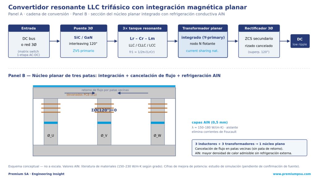
The schematic below places the full conversion chain and anticipates where power density is won: the integrated planar magnetic core.
Three-phase resonant converters and planar magnetic integration

Three-phase resonant network topologies

The dominant high-frequency topologies are LLC, CLLC and LCC, each with a distinct gain, impedance and bidirectional profile. In the LLC, each phase integrates a series resonant inductor (Lr), a series capacitor (Cr) and the transformer’s parallel magnetizing inductance (Lm); below the resonant frequency, Lm participates and provides a boost capability. The resonant frequencies are governed by fr1 = 1/(2π·√(Lr·Cr)) and fr2 = 1/(2π·√((Lr+Lm)·Cr)), and the inductance ratio is m = Lm/Lr; operating fs near fr1, the converter reaches its peak-efficiency point with unity gain.

Table 1 — Comparison of resonant topologies (traced to literature).

Topology Soft switching Bidirectionality Gain range Typical application
LLC Full primary ZVS; secondary ZCS below resonance Asymmetrical; high reactive current in reverse Moderate; strongly load-dependent far from resonance Unidirectional EV chargers, server/telecom PSU
CLLC Symmetrical ZVS in both power-flow directions Completely symmetrical (dual tanks) Wide; optimized for variable battery voltage Bidirectional EV chargers, V2G interfaces
LCC ZVS over a wide range down to zero load Asymmetrical (Cp alters reverse gain) Exceptionally wide; excellent at light load High voltage, capacitor charging, wide-range adapters
SRC Primary ZVS above resonance Symmetrical Narrow; gain strictly bounded below unity Fixed-ratio DC-DC, narrow-range bus converters

On the primary connection, the delta option (Δ-Cr) reduces the tank current by a factor of √3 —cutting the winding copper loss to one third versus the parallel star— but imposes a penalty: the volt-second stress on the high-frequency transformer also rises by √3.

Floating star (Y-primary) and natural current sharing

The most common configuration connects the three transformer primaries in a star with a common floating neutral point. This connection dynamically modulates the neutral-node voltage, reshaping the resonant currents toward a more rectangular than sinusoidal waveform: by flattening the peaks, it lowers the peak and RMS current versus a single-phase converter of equal power, reducing conduction losses. More importantly, it provides a natural current-balancing capability far superior to independent parallel converters.

Self-compensation and MTBF. Under resonant-capacitor tolerance or degradation (a common failure mode in high-temperature environments), the floating neutral shifts dynamically to accommodate the drift, preventing localized thermal runaway on an ageing phase. This passive, zero-cost balancing limits the mean current mismatch to under 15 % without any active control, and extends system MTBF.

Current imbalance and active mitigation

Despite the star node’s natural balancing, passive-component manufacturing tolerances (typically ±10 %) shift each phase’s impedance and produce thermal asymmetry and extra output-capacitor ripple. Hardware solutions (balancing transformers) add loss and volume, so active control is preferred:

  • CPAB (Current Phase Angle Balancing): directly regulates the phase angles of the resonant currents with dedicated PI loops to hold an exact 120° spatial displacement, limiting residual mismatch to under 5 % even under severe tolerances. It outperforms the historical TCB (Trigonometric Current Balancing), which has poor transient response.
  • RMS-based real-time algorithm: measures the individual RMS currents and linearly adjusts the input-voltage phase shifts (V and W channels relative to the U reference), reducing the imbalance factor to under 2 % across the full frequency range.
  • Phase-Shift Modulation (PSM): in two-module parallel three-phase structures, PFM regulates voltage and PSM shares current; a 30° displacement between modules minimizes total output ripple.

Stable implementation demands careful loop design: in a reference application, the voltage loop (PFM) uses a PI compensator with a 5 kHz crossover and 96° phase margin, while the current-sharing loop (PSM) uses integral compensators with a lower 500 Hz crossover and 91° margin to avoid loop interaction. With a physical mismatch of LrA=20 µH and LrB=16 µH, without active sharing the phase shifts lock at an identical 40.5°; with PSM active the controller dynamically diverges them (41.8° and 39.2°) and restores current symmetry.

Hybrid PFM + PSM modulation

Conventional PFM control varies the switching frequency to regulate voltage, but very wide voltage ranges (an EV charger may span 200 V to 1000 V) force it to sweep a huge frequency spectrum, complicating the EMI filter, drivers and magnetics, and increasing circulating-current losses far from resonance. The hybrid scheme uses PFM below resonance (boost mode, high efficiency) and activates PFM+PSM above it: shifting the phase angle between legs generates a three-level voltage waveform that adjusts the tank’s effective excitation, minimizing the frequency range and reactive circulating energy. The VCR-based VFSHC variant switches modes without transients and completely eliminates the «inoperative region» of conventional hybrid schemes.

Planar magnetic integration: three in one

The main drawback of three-phase is the escalation of magnetic components: three independent inductors and three transformers raise volume, cost and assembly complexity. Planar integration merges them into a single structure. Splitting the primaries across the legs of a three-column core, the sum of the 120°-shifted fluxes cancels in the center leg, which dramatically reduces core losses and simplifies thermal management. With WBG semiconductors (SiC/GaN) the frequency rises to the 500 kHz–1 MHz+ range, enabling PCB copper windings and very low-profile planar cores.

Not all geometries are equal. The classic square integrated core suffers asymmetrical reluctance paths —the center leg is shorter than the outer ones— which induce phase imbalance. An elegant spatial solution is the cylindrical planar core, which enforces complete three-dimensional symmetry and aligns the reluctances of the three phases. For very high currents, the matrix transformer (series primaries, parallel secondaries) distributes voltage stress and heat dissipation.

Table 2 — Planar magnetic integration strategies (traced to literature).

Strategy Core complexity HF loss reduction Reluctance symmetry Engineering challenge
Discrete parallel cores Low (standard cores) Low (no flux cancellation) High (independent paths) Large volume, low density, high cost
Square integrated core Moderate (single E-core) Moderate (center-leg cancellation) Low (outer legs longer) Asymmetry → phase imbalance
Cylindrical symmetrical core High (custom geometry) High (optimized uniform flux) High (complete 3D symmetry) Custom manufacturing and winding
Matrix transformer High (multi-core series-parallel) High (distributed core volume) High (symmetrical PCB routing) High secondary leakage inductance; routing

Core thermal management at 1 MHz: the role of AlN

As frequency rises to 1 MHz, ferrite core losses grow and push planar components toward their thermal margins. The reflex of inserting a metal piece (copper, aluminium) to cool the transformer internally is counterproductive: the alternating magnetic field induces severe eddy currents in the metal, sending losses up. The solution is a material that conducts heat but insulates electrically: aluminium nitride (AlN).

AlN combines a high thermal conductivity —on the order of 150–180 W/(m·K), and up to 230 W/(m·K) in premium commercial grades, comparable to some metals— with high dielectric strength. It is also 7 to 10 times the thermal conductor of alumina (Al₂O₃, ~30 W/(m·K)), cheap but poor, and unlike beryllium oxide (BeO, ~260 W/(m·K)) it is non-toxic. Being a non-conductive ceramic, interleaving thin AlN plates (e.g., 0.5 mm) within the ferrite block stack creates internal conductive cooling channels without inducing parasitic currents, draining heat from the inner —typically hottest— regions and lowering the core’s peak temperature.

Rigour on the improvement figures. Thermal-optimization studies report that a 1 MHz ferrite core with embedded 0.5 mm AlN layers would admit an increase on the order of 167 % in its admissible heat-generation density (theoretical models in the 173–187 % range), and that dedicating 30 % to 35 % of the core volume to AlN would maximize the sustainable useful flux. These specific figures could not be verified against independent public literature and are carried over as a simulation-study datum pending source confirmation; the AlN material properties are supported by materials literature. Recommendation: validate experimentally before publishing the improvement figures as a closed datum.

WBG semiconductors: the enabler and its constraints

High-frequency operation is made possible by wide-bandgap semiconductors. Versus silicon (Eg 1.1 eV, critical field 0.3 MV/cm, mobility 1400 cm²/V·s), SiC (3.3 eV, 3.0 MV/cm, 900 cm²/V·s, excellent thermal conductivity) and GaN (3.4 eV, 3.3 MV/cm, 2000 cm²/V·s) allow thinner drift regions, lower Rds(on) and blocking voltages from 650 V (lateral GaN) to 1200 V+ (vertical SiC).

The price is demanding hardware design. dv/dt of hundreds of volts per nanosecond excites circuit parasitics, generating oscillations, EMI and instability. In E-mode GaN, with a narrow gate window (−10 V to 7 V) and low threshold (Vth < 2 V), gate crosstalk can trigger catastrophic false turn-on events. The designer must use gate drivers with active Miller clamp, Kelvin source connections and strictly symmetrical PCB layouts to suppress spikes and keep the soft-switching boundaries.

Validated prototypes

Industry has built and measured several platforms that confirm the architecture’s advantages:

Table 3 — Published prototypes (parameters and achievements, traced to literature).

Platform Topology f_sw Voltage / power Efficiency and achievement
30 kW EV charger Three-phase interleaved LLC (SiC) 135–250 kHz Vin 650–850 V; Vout 200–1000 V Peak > 98 %; full load > 97 %
10 kW high-density CLLC Three-phase CLLC High frequency 800 V DC bus Peak 97.5 %; cylindrical planar; minimal imbalance
500 W single-stage AC-DC Matrix switch + LLC 465–547 kHz Vin 100 V AC; Vout 130 V DC Peak 97 %; PF 0.99; THD 3.95 %
4 kW bidirectional Three-phase LCC High frequency 320 V ↔ 28 V battery Peak 92.2 %; range 0–12.5 A / 0–142 A
3.6 kW grid-tied Interleaved LLC Synchronous frequency 48 V output CPAB controller with verified stable sharing

Synthesis — Premium SA design criterion

Translated into project recommendations, the three-phase resonant architecture is ordered as follows:

  • Bidirectional → CLLC: for V2G and grid storage, CLLC over LLC guarantees symmetrical gain and identical soft-switching boundaries in both directions.
  • Passive balancing → floating star: in high power with expected ageing or tolerances, the floating Y node provides zero-cost balancing (<15 %) and drift self-compensation.
  • Fine balancing → CPAB software: for critical applications, CPAB alongside the floating node drives the mismatch below 5 % with no extra hardware.
  • Wide range → hybrid PFM+PSM (VFSHC): limits the frequency spectrum, optimizes the planar magnetics and avoids the inoperative region.
  • Density → planar magnetics + AlN: cylindrical or matrix cores to cancel flux and spread heat; AlN conductive cooling to raise the thermal limit at 1 MHz without inducing eddy currents.
  • WBG → disciplined layout: active Miller clamp, Kelvin source and PCB symmetry to tame SiC/GaN dv/dt.

Sources and traceability

Premium SA internal catalogue: block B4 (resonant and multilevel topologies, manual_avanzado_diseno), B8 (passive/magnetic components), B7 (advanced thermal management). Consistent with the Premium article «Multilevel Inverters» v1.0 (no overlap: that one covers the inverter stage; this one, the resonant DC-DC stage).

External technical literature (selection):

  • Three-phase architecture and control: studies on three-phase LLC/CLLC/LCC, current sharing, CPAB and hybrid PFM-PSM modulation (IEEE/MDPI/ResearchGate; Wolfspeed 30 kW SiC charger).
  • Planar integration: cylindrical symmetrical core and matrix transformers for high-frequency three-phase LLC (MDPI Energies; magnetic-integration thesis, White Rose).
  • AlN properties: materials data (Kyocera, Precision Ceramics, substrate manufacturers): λ 150–230 W/(m·K) by grade; alumina ~30 W/(m·K); BeO ~260 W/(m·K), toxic; CTE matched to Si.
  • AlN power-improvement figures: simulation study cited in the source material — pending primary-source confirmation before publication as a closed datum.


About Premium SA

Premium SA is a Barcelona-based manufacturer of electronic power converters for railway, industrial and energy applications. With more than 900 standard product designs and over 40 years of operational experience, Premium SA supplies DC/DC converters, DC/AC inverters, AC/AC frequency converters, battery chargers, rectifiers and UPS systems from 50 W to 72 kW.

The D2x / DFR methodology integrates topology, digital control and the magnetic-thermal architecture as coupled decisions from the conceptual phase, with a preference for custom solutions, WBG semiconductors and traceable experimental validation.

Premium PSU
Premium SA · Barcelona, Spain · info@premiumpsu.com · +34 932 232 685 · www.premiumpsu.com
Born in Barcelona, Powering the World
Design, calculation and simulation of planar transformers
Application Notes, Energy, Sin categoría

Design, calculation and simulation of planar transformers

PREMIUM SA · ENGINEERING INSIGHT · HIGH-FREQUENCY MAGNETICS · 2026

Loss physics, winding structures, parasitics, insulation standards and the open-source software ecosystem for high-frequency magnetics.

Premium PSU


Executive summary

The drive for higher power density, efficiencies above 98 % and ultra-thin profiles has pushed the transition from the conventional wire-wound transformer to the planar transformer: photolithographically etched copper traces on multilayer PCB or foils, coupled to low-profile ferrite cores. The change is not just form factor; it redefines high-frequency electromagnetic losses, parasitic dynamics and the validation methodology.

This article systematizes advanced planar-transformer design: the loss physics (skin effect, proximity and the Dowell model), turns-number optimization, the interleaved winding structures that control the magnetomotive force, leakage-inductance and inter-winding-capacitance management, experimental and finite-element validation, insulation-standard compliance, and the software ecosystem —with particular attention to the open-source tools that enable first-class engineering without proprietary licences, consistent with Premium SA’s preference for open, auditable software.

All figures and tools are traced: to peer-reviewed technical literature (application notes, DTU/Ouyang papers, IPC/IEC standards) and to verified open-source repositories. The formulas are the classic ones of the domain.

≈ ⅓Planar profile (~10.7 mm) versus 30–40 mm conventional
> 98 %Efficiency of the 1 kW / 1 MHz LLC with full integration
< 1 %Hybrid analytical-FEA model error vs 3D transient
−75 %Leakage inductance reduction with simple interleaving

Planar versus conventional: what changes

Conventional round-wire, Litz or foil transformers on PQ/ETD bobbins have severe limitations above 100 kHz, and winding variability introduces parasitic spread that hampers industrial repeatability. The planar replaces coils with copper traces on multilayer PCB or foils coupled to low-profile EQ/ER/E-LP cores. The most visible consequence is geometric; the most valuable, repeatability.

Table 1 — Conventional versus optimized planar transformer (traced to literature).

Parameter Conventional (PQ32/35) Planar (EQ38/8/25) Engineering implication
Profile height 30–40 mm ≈ 10.7 mm (≈ ⅓) Integration into very low-profile boards (brick)
Weight High ≈ 3× lighter Critical in transport and aerospace
Parasitic repeatability Low (high spread) Very high (photolithography) Enables precise tuning of LLC tanks
HF conduction losses High (inefficient packing) Low if Rac is optimized Better dissipation and overall efficiency
Prototyping flexibility Very high (rewind by hand) Low (any change = new PCB) Forces simulation before fabrication

That last row sets the method: since any minor change requires a new PCB, planar design does not allow bench trial-and-error. It demands rigorous analytical modelling and simulation before going to production.

Systematic design methodology

The move to planar is not the geometric replica of a wire transformer: it requires a structured flow that audits the electrical, thermal and mechanical specifications and adapts them to PCB physics.

Table 2 — Planar design workflow (eight stages).

Stage Key action Critical parameter
1 · Base-design audit Collect V, P, f, Lm, Llk, insulation, temperatures Thermal and electrical targets to replicate/improve
2 · Core and material Planar geometry (EQ/ER/E-LP) and ferrite (N87/N95/3C95/3F3) Balance hysteresis loss vs available height
3 · Number of turns Np, Ns from Faraday’s law and ΔB max Fewer turns → less copper but more core
4 · Copper thickness Size h according to skin depth δ Avoid oversizing (aggravates proximity)
5 · Stack-up P/S/shield sequence and interleaving Determines Llk, Rac and global losses
6 · Trace width Carry the DC and AC current density Keep ΔT within safety limits
7 · Electrical/thermal validation FEA or advanced analytics of HF losses and T Spot hotspots before fabrication
8 · PCB fabrication Vias, insulation slots, export Gerber Manufacturability and insulation compliance

Loss physics: skin, proximity and Dowell

Accurate conduction-loss calculation is the greatest challenge in HF magnetics. Two coupled phenomena govern it. The skin effect concentrates current in a surface layer of depth δ = √(ρ/(π·μ·f)); for copper at 70 °C it reduces to the practical rule δ ≈ 2.276/√f mm. The resistance increase from this effect is Rac/Rdc = ξ·[sinh(2ξ)+sin(2ξ)]/[cosh(2ξ)−cos(2ξ)], with ξ = h/δ the normalized thickness: when ξ > 2, the conductor centre barely conducts and thickening the copper stops helping.

The proximity effect is more damaging. When layers are stacked, the fields of neighbouring conductors induce cross eddy currents. Dowell’s model for the m-th layer adds a second term scaling with (m²−1), where m is the layer’s MMF factor. Because that term grows quadratically with layer position, losses in stacks with many continuous non-interleaved layers explode. And since real currents are PWM, not sinusoidal, the resistance must be evaluated over the harmonic spectrum —P_AC = Σ Rac(n·fs)·I²rms(n)—: high-order harmonics, with very small δ, dissipate a lot even at moderate amplitude.

The optimal number of turns. Increasing N lowers the flux density ΔB and, via Steinmetz (Pv = K·f^α·ΔB^β, with β≈2–3), reduces core losses; but it demands narrower traces or more layers, raising Rdc and, through Dowell’s m, Rac. The optimum is not to eliminate one term but to balance them: the absolute loss minimum occurs when the copper losses are held at a factor β_loss = P_copper/P_core of the ferrite losses. It is the designer’s analytical tuning criterion.

Winding structures: interleaving as the lever

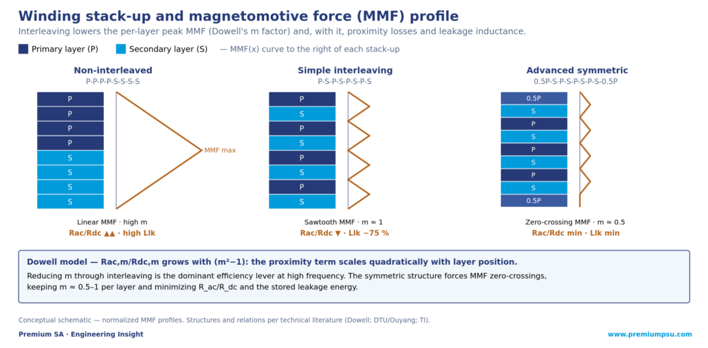
The way to tame proximity losses is to alter the spatial field distribution in the core window, abandoning simple non-interleaved stacks. Interleaving alternates primary and secondary layers with opposite current directions in adjacent layers, cancelling the net field and reducing Dowell’s m. The figure below compares three stack-ups and their MMF profile.

calculation
Figure 1 — Winding stack-up and MMF profile. Interleaving lowers the per-layer peak MMF and, with it, proximity losses and leakage.

The advanced symmetric structure 0.5P-S-P-S-P-S-P-S-0.5P —with the outer layers at half-turn and connected in parallel— forces multiple MMF zero-crossings, keeping m≈0.5–1 uniformly and minimizing both Rac/Rdc and the stored leakage energy. For fractional ratios or extreme thermal performance in the MHz range, the half-turn structure implements 180° traces in parallel on the outer layers, splitting the current and halving the peak field. And at high current, the interleaved serpentine winding snakes across several legs, maximizing window use without extra interconnection layers.

Table 3 — Winding structures and their behaviour (traced to literature).

Structure MMF profile Rac/Rdc Leakage Llk Routing / vias
Non-interleaved (P-P-P-P-S-S-S-S) Linear ramp; peak at interface Very high (accumulates m) Very high Minimal (no crossings)
Simple interleaving (P-S-P-S…) Sawtooth; moderate peaks Low (m≈1) Reduced up to −75 % High (alternating layers)
Advanced symmetric (0.5P-S…0.5P) Attenuated; cancellation at outer faces Absolute minimum (series-parallel) Very low and controlled Very high (parallel vias, symmetry)
Half-turn Shifted and symmetric to axis Very low (m≈0.5) Minimal for a given insulation Very high (fractional geometry)

Parasitics as design variables: leakage, capacitance and EMI

The planar’s tight spatial coupling maximizes mutual inductance but demands treating parasitics as active variables. Leakage inductance Llk arises from flux that closes through the window without linking both windings. In hard switching (full bridge, flyback) it is a harmful parasitic that causes overvoltages and demands snubbers; it is minimized with full interleaving and thin dielectrics. But in LLC resonant converters it is exploited: a controlled Llk is deliberately designed to act as the series resonant inductor Lr, removing a discrete component and gaining density. To tune it, magnetic shunts are inserted or the inter-layer dielectric spacing (Δh) is adjusted, which raises Llk linearly.

The high-frequency design dilemma. Reducing leakage forces primary and secondary close together, which raises the inter-winding capacitance C_inter. Under the primary’s fast dv/dt, C_inter injects common-mode displacement currents into the secondary, generating conducted EMI that demands bulky filters. It is broken with electrostatic shielding (a thin, slotted copper layer —to avoid shorting the flux— tied to a quiet ground) or with an auxiliary cancellation winding of opposite polarity (−dv/dt) that nulls the net common-mode current.

Validation: leakage measurement and hybrid analytical-FEA calibration

In a high-performance planar, Llk is under 1 % of the magnetizing inductance (often 0.1–0.2 %, in nanohenries), of the same order as the instrument leads’ own inductance. It is measured with the direct short-circuit method (a wide copper bar across the secondary + impedance analyzer at the decade of the switching frequency) or, without an HF analyzer, with the turns-ratio and AC-deviation method. In both cases it pays to build test fixtures with planar contacts and symmetrical coaxial traces to calibrate open/short at the device plane.

The one-dimensional Dowell model fails on real traces: concentric spirals concentrate the DC current at the inner radius (spirality effect), raising the real Rdc. The hybrid analytical-numerical methodology solves this without the cost of a full 3D transient: the ideal arc is computed (Rca = 2π/(σ·h_cu·ln(r₂/r₁))), the real resistance is extracted by static DC FEA with quarter symmetry, a calibration factor (Rca/R₊) is obtained and injected as a coefficient into the AC-loss formula. The result agrees with 3D transient simulations (Ansys Maxwell) within under 1 % error, in microseconds instead of hours.

Insulation and standards: clearance, creepage and IEC 60664-1

The proximity of high- and low-voltage traces demands strict compliance with dielectric standards. Clearance is the through-air distance (prevents direct arcing); creepage, the leakage path along the solid surface (prevents conductive carbonization). IPC-2221 sets minimums up to 500 V and adds a linear surcharge above that; IPC-9592, specific to power conversion, imposes more conservative criteria. High-CTI materials tolerate smaller creepages.

Distances are not read from a static table: IEC 60664-1 requires evaluating the real environment. The pollution degree (PD2 common in industry) can be reclassified to PD1 with conformal coating or potting, drastically reducing the required creepage. The overvoltage category (OVC) sets the primary clearance on mains. And altitude penalizes: above 2000 m the lower dielectric strength of air forces multiplying the clearance, with a factor of about 1.48 at 5000 m —relevant in mountain railway, high-altitude solar and avionics. Physically, creepage is multiplied by milling through slots in the FR4 between primary and secondary, forcing the leakage path to go around the cut, or by interposing insulating barriers.

Software ecosystem: open and commercial

The coupled complexity of the HF field has produced a mature software ecosystem. Premium SA prioritizes, where they meet requirements, open-source and auditable tools: they enable first-class engineering with no lock-in or licence cost, and their verifiable code fits the traceability that regulated sectors demand.

On the open side, the OpenMagnetics project stands out —a working group of the PSMA magnetics committee—: its MKF compute engine (C++) is exposed in Python via PyOpenMagnetics/PyMKF and operates on the neutral MAS format (Magnetic Agnostic Structure, a JSON schema describing requirements, construction and results, with insulation coordination per IEC 62368-1/61558). python-planar-magnetics (on PyPI) generates planar spirals respecting DRC rules, estimates Rdc correcting for spirality, and exports to KiCad (S-expressions) and DXF. For full FEA, ONELAB integrates Gmsh (meshing), GetDP (eddy-current fields coupled to SPICE) and Elmer (3D multiphysics in parallel, couplable to OpenFOAM for conjugate thermal). The Ansyas bridge (Synopsys–Würth collaboration) connects MAS to Ansys Maxwell via PyAEDT.

Table 4 — Software for planar magnetics design (verified).

Suite Licence Base / environment Capability for planars
PyOpenMagnetics / MAS Open source (MIT) Python wrapper · C++ MKF engine Proximity/skin losses, MAS JSON schema, SVG plotting
python-planar-magnetics Open source Parametric Python scripting DRC spirals, Rdc correction, KiCad/DXF export
ONELAB (GetDP/Gmsh/Elmer) Open source (GPL) General-purpose FEA + SPICE Coupled 2D/3D eddy current and conjugate thermal (OpenFOAM)
Ansys Maxwell Commercial Reference 3D EM FEA Nonlinear hysteresis, bidirectional thermal-mechanical coupling
COMSOL / CST Commercial Multiphysics FEA / FEM-FIT-TLM Coupled multiphysics; fine EMC validation
PI Expert (Planar Builder) Commercial (Power Integrations) Automated cloud synthesis Stack-up, core, widths, clearance/creepage and Gerbers

Synthesis — Premium SA engineering recommendations

  • Tuned copper thickness: keep h ≤ 2δ at the working frequency; in the MHz range, thin foils or 1–2 oz copper interleaved, never generic heavy copper.
  • Always interleave the stack: avoid continuous MMF ramps; prioritize symmetric structures (0.5P-S…0.5P) or half-turn to minimize proximity and leakage.
  • Parasitics by topology: in LLC, design Llk as the resonant inductor (removes the discrete part); in hard switching, minimize Llk and break C_inter with electrostatic shielding to a quiet ground.
  • Hybrid analytical-FEA flow: calibrate the Rac equations with a geometric factor extracted from static DC FEA; enables Pareto optimization with <1 % error versus the 3D transient.
  • Insulation by real environment: size clearance/creepage with IEC 60664-1 (PD, OVC, altitude); mill slots in the FR4 and evaluate conformal coating to reclassify PD2→PD1.
  • Open software first: OpenMagnetics/MAS and python-planar-magnetics for synthesis and losses; ONELAB/Elmer for FEA; reserve commercial suites for final multiphysics validation.

Sources and traceability

Premium SA internal catalogue: block B8 (passive/magnetic components), B7 (thermal management), B4 (resonant topologies). Companion to the Premium article «Three-phase resonant converters and planar magnetic integration» (that one, system-level integration; this one, planar-transformer design methodology).

External technical literature and tools (selection):

  • Losses and design: Dowell model; loss and leakage optimization in planars (DTU / Ouyang); Texas Instruments application notes (Topic 4, Designing Planar Magnetics).
  • Case studies: 1 kW / 1 MHz one-eighth-brick LLC (TI SSZTD94); 1 W ultra-flat isolated supply TIDA-00688 (TI TIDUB83).
  • Insulation: IPC-2221 / IPC-9592; IEC 60664-1 (insulation coordination; altitude factor ≈1.48 at 5000 m); IEC 62368-1.
  • Open software (verified): OpenMagnetics / MAS / PyMKF (PSMA Magnetics Committee WG; IEEE-PELS, 40+ models); python-planar-magnetics (PyPI, dzimmanck); ONELAB / GetDP / Gmsh / Elmer; Ansyas bridge (Synopsys–Würth).


About Premium SA

Premium SA is a Barcelona-based manufacturer of electronic power converters for railway, industrial and energy applications. With more than 900 standard product designs and over 40 years of operational experience, Premium SA supplies DC/DC converters, DC/AC inverters, AC/AC frequency converters, battery chargers, rectifiers and UPS systems from 50 W to 72 kW.

The D2x / DFR methodology integrates magnetic design —including parasitic co-design and simulation verification— from the conceptual phase, with a preference for open-source, on-premises and auditable tools, and traceable experimental validation compliant with the standards of regulated sectors.

Premium PSU
Premium SA · Barcelona, Spain · info@premiumpsu.com · +34 932 232 685 · www.premiumpsu.com
Born in Barcelona, Powering the World
Industrial Power Converter Selection Guide: 5 Critical Parameters
Application Notes

Industrial Power Converter Selection Guide: 5 Critical Parameters

Technical Guide · Industrial Power Electronics · Barcelona, Spain

Industrial Power Converter Selection Guide: 5 Critical Parameters

The parameters most engineers overlook when specifying an industrial power converter — and why they determine whether a design succeeds or fails in the field. Insights from 900+ designs delivered from Barcelona.

Premium PSU — Industrial power converter manufacturer in Barcelona, Spain
|
April 2026
|
For automation engineers, maintenance managers and industrial machinery designers
900+
Designs delivered
50 W–72 kW
Power range
4–6 wks
Lead time Europe
15–25 yrs
Target service life


Selecting an industrial power converter seems straightforward: define input voltage, output voltage, power rating, and find a supplier. In practice, most field failures with industrial power converters are not caused by equipment defects — they result from incomplete or incorrect specifications. This guide distils the selection criteria that more than 900 designs, delivered from our manufacturing facility in Barcelona, Spain, have taught us make the real difference.

The Five Parameters Everyone Specifies

Input voltage, output voltage, nominal power, efficiency and operating temperature. These are the basic parameters listed in any industrial power supply datasheet — well documented and universally understood. We will not dwell on them here.

What matters are the parameters that are routinely omitted, yet determine whether the industrial DC/DC converter — or inverter — will operate reliably throughout the entire service life of the installation.

The Five Parameters Most Engineers Overlook

1. Actual Input Voltage Range

Most specifications state the nominal voltage. In a real industrial environment, however, mains voltage can fluctuate between +10% and −15% of nominal. Switching transients can add spikes of several hundred volts. Specify the full range the power converter must tolerate — transients included.

2. Load Inrush Current

A 5 kW motor can demand 15 kW during the first seconds of start-up. A converter sized only for nominal power will trip on overcurrent. Specify peak power and its duration.

3. Real Ambient Conditions

Not the laboratory conditions — the actual installation conditions. Peak summer temperature inside the electrical cabinet (easily 55–60 °C with poor ventilation). Altitude (air density decreases above 1,000 m, reducing cooling capacity). Humidity, dust, vibration. These factors are frequently underestimated in industrial installations across Southern Europe.

4. Electromagnetic Compatibility (EMC)

In industrial environments with variable-speed drives, welding equipment and large motors, electromagnetic interference levels are significant. An industrial inverter without adequate EMC filtering can cause malfunctions in nearby PLCs and sensors. In Europe, compliance with EMC Directive 2014/30/EU is mandatory for equipment in service.

5. Galvanic Isolation

In many applications, electrical separation between input and output is not a feature — it is a safety requirement. Specify the isolation voltage required (typically 1,500 Vdc or 3,000 Vdc for industrial applications). This is especially relevant in railway, energy and defence sectors.

Golden rule: A complete technical specification reduces field incidents by more than 70% during the first 12 months of operation. Time spent on correct parameter definition is always less than the cost of a field replacement for an industrial power converter.

Common Errors in Industrial Power Converter Selection

Error Description Real impact
Error 1 Sizing for nominal power without accounting for inrush peaks Overcurrent trips. Practical rule: size at least ×1.5 nominal power when motor loads are present.
Error 2 Ignoring thermal derating A 10 kW converter rated at 25 °C ambient may deliver only 7 kW at 55 °C. Always consult the manufacturer’s derating curve and calculate for your actual operating temperature.
Error 3 Selecting on unit price The cost of a field failure (production downtime, technician dispatch, spare parts, lost revenue) is typically 5 to 20 times the equipment price.
Error 4 Not verifying long-term product availability Industrial equipment is installed for 15–25 years. A product discontinued after 5 years can trigger a redesign costing over €30,000 per affected model.

Standard vs. Custom Industrial Power Converter: When to Choose Each

Standard converters cover the majority of common industrial applications and offer the best cost-to-lead-time ratio. There are, however, situations where a custom industrial power converter is the right choice:

  • When physical space is critical (standard enclosure does not fit the cabinet or machine).
  • When multiple outputs at different voltages are required from a single input.
  • When environmental conditions are extreme (temperature, vibration, corrosive atmosphere).
  • When volume justifies an optimised design (typically from 50–100 units per year).
Premium SA approach — Configurable platforms: a proven, certified base design with adjustable parameters (input voltage, output configuration, mechanical enclosure, environmental protection). Manufactured in Barcelona, Spain. This delivers 80% of the benefits of a fully custom design at 20% of the engineering cost — with competitive lead times across Spain and Europe.

Industrial Sectors We Serve in Spain and Europe

From our manufacturing plant in Barcelona, Spain, we supply industrial power converters to sectors including industrial automation, defence, telecommunications, renewable energy, electrical grid infrastructure and railway. Customers such as iGRID (battery chargers for electrical infrastructure, 100+ units/year), INDRA (converters for railway signalling systems), Iberdrola (inverters for distribution installations) and multiple industrial OEMs across Spain and Europe rely on our equipment for their most demanding applications.

The advantage of working with a specialised European power converter manufacturer is clear: 4–6 week lead times in Spain and Europe, direct technical support from the engineering team that designed the product, and the flexibility to adapt solutions without the lead times or costs of large multinational groups.

Do you need an industrial power converter for your application?

Describe your project and our engineering team in Barcelona will recommend the optimal solution. We manufacture industrial power converters from 50 W to 72 kW. Delivery in 4–6 weeks across Spain and Europe.

Contact our technical team in Barcelona →

You may also be interested in:

  • Industrial DC/DC converters
  • DC/AC inverters for industrial applications
  • Industrial battery chargers
  • Frequency converters for export manufacturing


Premium PSU — Industrial power converter manufacturer in Barcelona, Spain
Born in Barcelona, Powering the World · premiumpsu.com
What is an Electronic Fuse (eFuse) and Why Is It Replacing Conventional Fuses in Industrial Panels?
Application Notes, Energy

What is an Electronic Fuse (eFuse) and Why Is It Replacing Conventional Fuses in Industrial Panels?

Engineering Insight · eFuse

What is an Electronic Fuse (eFuse) and Why Is It Replacing the Conventional Fuse in Industrial Control Panels?

By the Premium PSU technical team · May 2026 · Reading time: 7 minutes


Born in Barcelona, Powering the World

45 min
Diagnosis with conv. fuse
<8 min
Diagnosis with eFuse
−82%
Diagnosis time reduction
10–100 µs
MOSFET switching time

ENGINEERING INSIGHT

What is an electronic fuse (eFuse) and why is it replacing the conventional fuse in industrial control panels?

By the Premium PSU technical team · May 2026 · Reading time: 7 minutes

Keywords: electronic fuse, eFuse, DIN rail, control panel, selective protection, electrical enclosure

Inside any industrial control panel, hidden among terminal blocks and PLCs, there are dozens of conventional fuses. For decades they have served a simple purpose: to blow when the current exceeds the rated limit. Yet that protection model — passive, slow and silent — is becoming obsolete in the face of modern automation system requirements.

The electronic fuse, also known as an eFuse or Electronic Circuit Breaker (ECB), does not blow. It detects overcurrent in microseconds, switches off the circuit electronically, indicates which channel has faulted via LED or digital signal, and can reset automatically once the root cause of the fault has cleared. This article explains how it works, when to apply it, and which parameters to evaluate when selecting the right model.

A counterintuitive technical decision: an eFuse costs between €12 and €25 per protected channel versus €0.50–2.00 for an equivalent conventional fuse. The paradox is that the eFuse proves more cost-effective in any installation that experiences more than 3–4 circuit faults per year. The reasons lie in the real cost of each intervention, not in the price of the component.

  1. The real problem with conventional fuses

A conventional fuse does exactly what its name implies: it melts to interrupt the circuit. This simplicity carries a cost that rarely appears in the distributor’s catalogue:

  • High diagnosis time: when a fuse blows, the operator must identify which of the many fuses in the panel has failed, test each one with a checker or inspect them visually, locate the correct spare in stock, and reinstall it. In a panel with 50 circuits, this process can take 20–60 minutes.
  • No indication of root cause: a blown fuse gives no information about whether the fault was a momentary short circuit (electromagnetic noise, inrush current) or a sustained overload pointing to a real load defect. The technician does not know whether to reset or whether there is an underlying fault to repair.
  • No automatic selectivity: if the trip current is not properly coordinated with the PSU characteristic curve and the other protective devices, the upstream fuse may blow before the one protecting the faulty branch, causing a wider outage than necessary.
  • Spare parts inventory cost: every fuse rating (0.5 A, 1 A, 2 A, 4 A, 6 A, 10 A…) requires stocking spare units. In installations with many different ratings, managing the spares inventory consumes time and money.

The combined effect of these factors makes the conventional fuse a significant source of operational cost in industrial installations with high-density 24 VDC circuits.

  1. How an electronic fuse works

An eFuse is essentially a controlled electronic switch. Its basic architecture combines three elements:

  • Power MOSFET: acts as the switching element. When the controller detects an overcurrent, it turns the MOSFET off in microseconds (typically 10–100 µs), with no electrical arc and no mechanical wear.
  • Integrated current sensor: continuously measures the output current of each channel. The measurement is analogue or digital (resistive shunt + ADC) with sufficient resolution to distinguish between a mild overload, a severe overload, and a short circuit.
  • Controller with configurable trip logic: compares the measured current against the user-set threshold (via potentiometer, DIP switch, or digital interface) and triggers channel opening when the limit is exceeded, following the desired time curve (instantaneous for short circuits, time-delayed for overloads).

The complete trip sequence — detection, decision, and opening — takes less than 1 ms in most industrial models. A conventional 10 A fuse may take 10–100 ms to blow at 15 A; during that time, a faulty load may have sustained additional damage or propagated the fault to other components.

Comparative trip speed: a short circuit on a 24 VDC circuit protected by a conventional 4 A fuse (type gG) generates a fault current of 20–50 A for 10–40 ms before opening. The same scenario with a correctly sized eFuse is resolved in <1 ms. The difference in energy dissipated in the load is an order of magnitude.

  1. Operational advantages over conventional fuses

The eFuse’s superiority in industrial applications is not merely theoretical. It manifests across four concrete operational dimensions:

3.1 Instant diagnosis

Each eFuse channel has a status LED (green = OK, red = tripped) and, in models with IO-Link communication or a digital alarm signal, sends real-time status to a PLC or SCADA. The operator — or the supervisory system — knows within seconds which channel has failed without opening the panel. Average diagnosis time drops from 20–60 minutes to 2–5 minutes.

3.2 Reset without physical intervention

Configured in auto-reset mode, the eFuse closes the channel again automatically after a configurable wait time (typically 0.5–10 s). If the fault was transient — an inrush current spike, an electromagnetic interference event — the system recovers on its own. In manual reset mode, the operator presses a button with no need to replace any component.

3.3 Selective protection without complex coordination

The trip current is adjusted channel by channel, with a precision of 0.1–1 A depending on the model. There is no need to calculate coordination curves between cascaded fuses because the eFuse protects only its own channel and does not interfere with the others. A short circuit on channel 3 does not affect channel 4, even if both are powered by the same PSU.

3.4 Elimination of spare parts inventory

A single multichannel eFuse module protects 4 or 8 circuits with different loads. There are no spare fuses to manage, sort, or order urgently in the middle of the night during a plant breakdown. The module has a typical service life of 10+ years with no maintenance.

  • Reference figure: Murr Elektronik quantifies in its product documentation (2024) an average 60–80% reduction in fault diagnosis time for 24 VDC circuits when replacing conventional fuses with LED-signalling eFuses. For installations with 50+ circuits, this saving represents between 200 and 600 technician-hours per year in the most demanding cases.
  • Applications where the eFuse delivers the greatest value

Not all installations justify the investment in eFuses equally. The applications with the highest return are:

  • High-density circuit control panels: automation enclosures with 20 or more 24 VDC circuits powering different loads (sensors, valves, actuators, drives). Density justifies channel-by-channel selective protection.
  • Continuous production lines: in manufacturing where every minute of downtime has a direct economic cost (€200–2,000/hour depending on the sector), the eFuse’s automatic reset can restore the system without human intervention and without stopping production.
  • Data centres and server rooms: 24 VDC control circuits for IT equipment (PDUs, KVM switches, temperature sensors, UPS systems) demand maximum availability. The eFuse with alarm signal enables integration with Data Centre Infrastructure Management (DCIM) systems.
  • Food and beverage OEM machinery: environments with washdown cycles and high humidity where corrosion degrades conventional fuses prematurely. The eFuse, with no mechanical parts, is far more robust in these conditions.
  • Solar energy and storage systems: inverters and control systems in photovoltaic installations require protection of auxiliary low-voltage DC circuits (24 V) against faults that could compromise system availability for hours.
  • How to choose the right eFuse: five key parameters

Selecting an industrial eFuse requires evaluating five parameters in the order indicated:

  1. The Premium PSU eFuse range

Premium PSU launches its first range of electronic fuses for DIN rail in 2026, designed specifically for the Spanish and Portuguese markets with local technical support in both languages. The range includes 1- and 4-channel modules for 24 VDC with per-channel adjustable current from 1 to 10 A and a rail width competitive with the best on the market.

Unlike higher-volume manufacturers, Premium PSU combines in a single offer the DIN Rail PSU for power supply and the eFuse for selective protection, with a unified warranty and a single technical-commercial contact for the complete panel. Technical documentation and application diagrams are fully available in Spanish.

  • Premium PSU is the only manufacturer simultaneously offering DIN Rail PSU + eFuse with native technical support in Spanish and Portuguese, with field presence in Spain and Portugal. Customers with ongoing projects can request evaluation samples at no charge by contacting their regional sales representative.

The electronic fuse is not an emerging technology; it has been present in the European industrial market for more than a decade and is available in the catalogues of the leading automation manufacturers. What is changing in 2025–2026 is the context: the digitalisation of control panels, the demand for greater production line availability, and the growth of new applications such as data centres and solar energy are transforming the eFuse from an interesting technical option into a standard component in modern projects.

For panel builders and OEMs still designing with conventional fuses, the question is not whether the eFuse is technically superior — it is, in virtually every relevant technical parameter. The question is whether the additional cost per channel is justified in their specific application. The next article in this series answers that question with real figures: a comparative 5-year TCO analysis for an industrial panel with 50 DC 24 V circuits.

Would you like to evaluate whether the eFuse is right for your next project? Contact the Premium PSU technical team: info@premiumpsu.com

PREMIUM PSU · Power supplies equipment and systems · www.premiumpsu.com

# Parameter Typical range What to evaluate
1 Output current per channel 0.5 A — 20 A Size to 125% of the load’s rated current. Leave headroom for motor and valve inrush current peaks.
2 Number of channels 1 / 2 / 4 / 8 In high-density panels, prioritise multichannel modules. An 8-channel module occupies 48–80 mm on DIN rail versus 8 individual fuse holders.
3 Rated input voltage 24 VDC / 48 VDC Most eFuses on the market are optimised for 24 VDC. For 48 VDC, verify the model’s input voltage range.
4 Communication and diagnostics None / LED / IO-Link / digital signal For systems without PLC or SCADA: LED is sufficient. For automation integration: IO-Link or digital alarm signal with PLC output.
5 DIN rail width 6 – 90 mm / 4 channels In space-constrained panels, width is decisive. The best models on the market achieve 6–8 mm per channel.
About Premium SA: Founded in Barcelona, Premium SA designs and manufactures
custom high-reliability power supplies and protection systems for industrial automation,
energy, and critical applications.
Over 40 years of experience in custom power electronics.www.premiumpsu.com ·
Contact our engineering team →

Premium SA — Born in Barcelona, Powering the World

Do you need a DIN Rail power supply or eFuse for your project?

Our applications engineering team responds in under 24 h. No commitment required.

Contact the team
View product catalogue
Thermal Design in Power Electronics
Application Notes

Thermal Design in Power Electronics


Engineering Insight · Technical Article · DFR · custom power supplies”>RDi

Thermal Design in Power Electronics

From thermal budget and Arrhenius law to active temperature management: DFR methodology and concurrent design in SiC/GaN converters

Premium PSU
|
Premium SA · Barcelona
|
April 2026
|
#PowerElectronics #ThermalDesign #SiC #GaN #Reliability #DFR #PremiumPSU
55%Failures of thermal origin
×2Failure rate per 10°C
3–5×Bond cycles lost per 30%ΔTj
100×Redesign cost at qualification


Executive Summary

Temperature is, without question, the most critical state variable for the reliability of a power electronics converter. Industrial surveys converge on a figure that no engineer should ignore: approximately 55% of premature electronic failures have thermal origin. Behind that percentage is not a single mechanism but a cascade of physical phenomena — thermo-mechanical fatigue from CTE mismatch, accelerated electromigration, dielectric breakdown, creep in bonding materials — all of which accelerate with temperature and, worse still, with its cyclic variation.

The consequence is direct: thermal design cannot be treated as an afterthought. The obsolete practice of closing the schematic and “adding a fan at the end” multiplies the redesign cost between 10 and 100 times. This article translates the fundamentals of modern thermal design into the language of the power converter designer: thermal budget, derating, cooling technology hierarchy, and the transition from “reactive” to “concurrent” design that Premium SA has integrated into its DFR methodology.

1. The Physics Behind the 55% — What Temperature Destroys

1.1 The Arrhenius Law

The most powerful practical rule in thermal design is the Arrhenius law applied to useful life: for every 10 °C increase in Tj, the component failure rate doubles, reducing its useful life roughly by half. Conversely, every 10 °C reduction doubles the life. The mathematical formula is L(T) = L₀ · exp[Ea/k · (1/T − 1/T₀)], where Ea is the activation energy of the degradation mechanism (typically 0.7–1.2 eV in power electronics; 0.94 eV for aluminium electrolytic capacitors per JEDEC).

The Arrhenius arithmetic. Equipment that routinely operates its semiconductors at 95% of Tj_max will fail in a fraction of the operational horizon of equivalent equipment with derating to 75–80%, even though the latter costs 10–20% more in BOM from oversizing the thermal path. In critical infrastructure with 30-year horizons, thermal derating is not optional — it is the most cost-effective capital investment in the design.

1.2 Thermo-Mechanical Fatigue — CTE Mismatch as the Dominant Mechanism

If Arrhenius governs degradation at constant temperature, the Coffin-Manson model governs degradation at variable temperature. In any power module, materials with very different CTEs coexist: the silicon chip (≈ 3 ppm/K), the DBC ceramic substrate (Al₂O₃ ≈ 7 ppm/K, AlN ≈ 4.5 ppm/K), the copper metallisation (≈ 17 ppm/K), the SAC305 solder. When temperature rises and falls, each material expands and contracts at its own rate, and the interfaces absorb the mismatch as cumulative plastic deformation. Coffin-Manson establishes that for every 30% increase in ΔTj amplitude, the wire bonds of the module lose a factor of 3 to 5 in cycles to failure.

1.3 Other Temperature-Accelerated Mechanisms

Electromigration — at high current densities and elevated temperatures, electrons drag metal atoms. Dominant model: Black, MTTF ∝ J−2·exp(Ea/kT). TDDB (Time-Dependent Dielectric Breakdown) — traps in the MOSFET gate oxide accumulate until they create a conduction path and catastrophic failure. NBTI/PBTI — hydrogen diffusion in the gate oxide, gradual Vth degradation. Creep — slow plastic deformation in bonding materials of heavy passive components.

Above all these gradual mechanisms is the absolute limit: when Tj exceeds the manufacturer-specified maximum (150 °C for Si, 175–200 °C for SiC, up to 250 °C for some GaN), the device is destroyed instantaneously and irreversibly.

2. The Thermal Budget — The Electrical Analogy

The central analytical instrument of thermal design is the electrical-thermal analogy: temperature → voltage, heat flow → current, thermal resistance → resistance. ΔT = Q · Rth. Junction temperature in steady state is: Tj = Ta + Q · (Rth(j-c) + Rth(c-h) + Rth(h-a)).

2.1 Worked Example — SiC Module in Railway Traction Inverter

Case: 1200 V/100 A SiC module in traction inverter. Ta_max = 70 °C; Premium SA derating at 80% of Tj_max = 175 °C → Tj_design = 140 °C; Q = 250 W. If the thermal budget calculation yields Tj = 145 °C, this exceeds the design objective by 5 °C. This is a budget failure that must be addressed at schematic stage: improving the cold plate, reducing Q via lower fsw, or paralleling modules. Ignoring the calculation and discovering the problem in qualification is not admissible.

2.2 Transient Modelling — Foster / Cauer Networks

The steady-state thermal budget grossly overestimates temperatures under variable load profiles. Transient modelling incorporates thermal capacitance Cth (the material’s capacity to store heat before transmitting it). Foster networks — cascaded Rth-Cth pairs — are the standard format in manufacturer datasheets. The practical consequence: a module can absorb short power peaks without Tj rising to the steady-state prediction value — enabling significantly reduced heatsink sizing in applications with pulsed duty cycles.

3. The Cooling Technology Hierarchy

The golden rule: always use the simplest solution that meets the thermal requirement. Each step up in the cooling hierarchy adds cost, mechanical complexity, and additional failure modes. The selection criterion is set by the surface heat flux density Q/A in W/cm².

Technology Max Q/A (W/cm²) Typical application
Natural convection < 0.3 Low-power, signal electronics
Forced air cooling 0.3 – 2 Standard rack converters, UPS
Liquid cold plate 2 – 50 Railway traction inverters, high-power industrial
Nucleate boiling 50 – 200 High-power prototypes, aerospace
Liquid microchannels 200 – 790+ AI/OCP servers, future high-density power modules

3.1 Why SiC/GaN Does Not Relax the Thermal Problem

A frequent — and incorrect — intuition holds that the transition to WBG semiconductors simplifies cooling. SiC and GaN are more efficient, have higher Tj_max, and operate at higher frequencies: three genuine gifts. But the chip is 4–10× smaller than its silicon equivalent for the same current rating, concentrating the heat flux in a much smaller area.

The National Renewable Energy Laboratory has quantified this effect: in simulations of automotive inverters with SiC operating at Tj = 250 °C, DC bus capacitors exceed 130 °C — more than 40 °C above the typical limit of polypropylene capacitors. SiC does not relieve thermal management: it transfers it from the chip to the rest of the inverter.

4. From Reactive to Concurrent Design

The historical reactive approach — close the schematic, lay out the PCB optimising only electrical criteria, and add a fan if temperature rises — carries a well-known structural cost: every thermally-detected problem triggers a redesign cycle whose cost scales as 1× at schematic, 10× at layout and 100× at qualification.

The modern paradigm — integrated into Premium SA’s DFR methodology — is concurrent design. Electrical, mechanical and thermal evolve in parallel, with cross-criteria from the first schematic trace. Component placement in the layout simultaneously obeys three logics: electrical signal integrity, mechanical integrity, and thermal separation between heat sources.

What changes with concurrent design: The heatsink is designed at the same time as the schematic, not after. Components with lower thermal tolerance are placed outside the “thermal wakes” of power dissipators. The thermal budget is calculated before fabricating any PCB. Failures are found in models, not on test benches.

5. Hierarchical Thermal Modelling

Level Tool Time Use
Level 1 Analytical models, Rth networks Minutes Rule out unviable architectures, compare cooling options
Level 2 Simplified 2D simulation Hours Optimise layout, study gradients in critical zones
Level 3 Full 3D CFD, refined mesh Days Final design validation before prototype
Level 4 Experimental (IR, thermocouples) Weeks Physical prototype validation, model feedback

The operational rule: never launch a level without exhausting the previous one. Analytical models eliminate 80% of options; 2D refines to 2–3 candidates; CFD validates the final one.

6. The Complete Thermal Chain — TIM, Substrates, Heatsinks

However sophisticated the cooling, heat only evacuates as far as the weakest link in the thermal chain allows. The thermal budget is distributed across all stages, and any of them can become the bottleneck.

6.1 Thermal Interface Materials (TIM)

TIM κ (W/m·K) Premium SA notes
Standard silicone grease 1–3 Outgassing and migration risk in railway cabins with optical sensors
Advanced ceramic pads 6–10 Current industrial standard
PCM metallised pads (phase-change) >12 Premium SA standard in railway programmes with silicone restriction
Dispersed graphene TIM ~30 Next generation — qualification in progress 2026–2027
Gallium-based liquid metals 50–80 Al compatibility challenges; high-power prototypes
Vertically-aligned CNT >100 Research frontier — not yet industrial maturity

6.2 DBC Ceramic Substrates

Substrate κ (W/m·K) CTE (ppm/K) Positioning
Al₂O₃ (alumina) 24–26 7.0 Cost-optimised industrial applications
Si₃N₄ (silicon nitride) 70–90 ≈ 2.7 CTE near Si; gaining share in railway with severe thermal cycling
AlN (aluminium nitride) 150–180 4.5 Dominant in railway traction, industrial SiC
Diamond DBC >1,000 1.5 Research / aerospace — cost barrier for industrial

Si₃N₄ is gaining market share because its CTE (≈ 2.7 ppm/K) is very close to that of silicon (≈ 3 ppm/K), drastically reducing CTE mismatch at the die-substrate solder interface and — via Coffin-Manson — multiplying module life under severe thermal cycling. AlN still dominates for pure κ, but Si₃N₄ is now the preferred choice in railway programmes where thermal cycling fatigue is the dominant failure mechanism.

7. Active Thermal Management — The Lever Available Today

While advanced materials mature, the lever with the best cost/benefit ratio available today is software-based active thermal management (Andresen and Liserre, Microelectronics Reliability, 2014). The controller firmware can significantly reduce ΔTj amplitudes without touching module hardware through four techniques:

Four active thermal control techniques.
(1) Adaptive fsw modulation — reduced during power transients to lower switching losses, with acceptable transient THD increase.
(2) Loss redistribution between parallel phases — the controller identifies the module with the highest Tj (estimated in real time) and shifts current towards less stressed ones.
(3) Real-time Tj estimation — from Vce_sat or RDS(on) measured during switching, reconstructing Tj without additional sensors.
(4) Accumulated cycle counting — firmware tracks power cycles and their associated ΔTj, enabling RUL (Remaining Useful Life) prognosis on wire bonds and solder joints.

8. Synthesis — Thermal Design as a Strategic Decision

Modern thermal design in power electronics rests on five concrete pillars that every Premium SA programme must satisfy:

Pillar What it guarantees
1. Thermal budget at schematic Tj < Tj_design = 0.80 × Tj_max under worst-case mission profile
2. Transient modelling Realistic heatsink sizing for pulsed duty cycle applications
3. Concurrent design Layout simultaneously optimised for electrical, mechanical and thermal integrity
4. Optimised TIM–substrate–heatsink chain No bottleneck at any link in the thermal chain
5. Active thermal management ΔTj reduction by software → 2–5× life extension with no BOM change


About Premium PSU

Premium SA is a Barcelona-based specialist in custom power electronic converters for railway, industrial, defence, and energy applications. The DFR (Design for Reliability) methodology integrates thermal design as a fundamental pillar from the conceptual phase of every project. Born in Barcelona, Powering the World.

www.premiumpsu.com · info@premiumpsu.com · +34 932 232 685

Premium PSU
© 2026 Premium SA · www.premiumpsu.com
Engineering Insight · Technical Article · DFR · RDi · April 2026

Premium SA — Born in Barcelona, Powering the World

Need a custom power supply for your critical application?

Our engineering team designs custom power electronics solutions for railway, defence, energy and industrial applications.

Contact our engineering team
View product catalogue
Ezequiel Navarro
Application Notes

Barcelona, the epicentre of the AI energy revolution.

Opinion · AI & Energy

Barcelona, the epicentre of the AI energy revolution. Where is Spanish industry?

A view from the OCP EMEA Summit 2026 — and a message to the Spanish industrial base of pumps, heat exchangers, valves and fluid systems

By Ezequiel Navarro, CEO — Premium S.A.  ·  30 April 2026

Premium SA
Born in Barcelona, Powering the World
85%
Energy share of data-centre OPEX
7–8%
Projected global electricity use, 20-yr horizon
800 VDC
Sidecar bus consensus
100–300 kW
Rack density — liquid cooling mandatory

This week, the Centre de Convencions Internacional de Barcelona has hosted the OCP EMEA Summit 2026. Two days. Hundreds of engineers, executives and technology leaders from the largest companies on the planet: NVIDIA, Microsoft, Schneider Electric, AMD, Oracle, ABB, Eaton. And me, walking the aisles with a growing certainty that what is being decided here is not only the design of the next data centre. What is being decided is how the world is going to consume — and manage — energy over the next two decades.

Let me explain why that matters. And why it matters especially if you design or manufacture pumps, heat exchangers, industrial fluid systems, or anything related to the transfer of thermal energy.

The consensus arrived sooner than expected

Eighteen months ago, the 800 VDC bus in data centres was an advanced technical bet — an attractive but speculative roadmap. This week, in a room full of hundreds of industry engineers, Schneider Electric framed it in a single sentence that will resonate across the industry:

“The sidecar is the immediate enabler of 800 VDC.”
— Schneider Electric, OCP EMEA Summit 2026

The sidecar — a power rack adjacent to the compute rack that converts AC to 800 VDC right on the data-centre floor — is now the architectural consensus of the industry. Not a speculative roadmap. A decision. Oracle puts it on its slides. Eaton has it as physical hardware on display in the Innovation Village. Microsoft is rolling it out across its new campuses. NVIDIA explicitly includes it among its four OCP contributions for data-centre efficiency.

For those of us who have spent years working in power electronics for critical applications — railway, defence, renewables — this shift has a particular flavour. The logic that defines the 800 VDC sidecar is exactly the same logic we have been applying for decades in railway traction: high-voltage bus, localised conversion, redundancy, real-time telemetry. The data-centre world is rediscovering what railway traction has known since the nineties. And the roadmap is clear: 1.2 MW sidecars in 2027, centralised DC distribution at 5 MW in 2028–2029, solid-state transformers at 10 MW in 2030.

Energy is the problem. Efficiency is the only way out.

NVIDIA presented at the summit two figures that ought to be on the front page of any European industrial plan for the next twenty years.

First: energy today represents 85% of the total operating cost of a data centre. Not the hardware. Not the software. Not the staff. Energy.

Second: data centres will go from today’s 1–2% of global electricity consumption to 7–8% over the next twenty years. For context: every interaction with ChatGPT consumes 500 ml of water. And the growth rate of AI models is not slowing down — it is accelerating.

If Europe does not act on efficiency, that growth will translate into energy dependence, unsustainable pressure on the grid and emissions impossible to offset. Every percentage point gained in the power-conversion chain — from grid to chip — has a direct and massive impact on the operator’s dominant budget line. OmniOn Power quantified it without ambiguity: 1 percentage point of efficiency improvement equals 2 MW saved per 100 MW of installed DC power, or roughly USD 250,000 per year per medium-scale installation.

That is why the entire industry is here, in Barcelona, talking about inductors, transformers, capacitors, GaN and SiC semiconductors, CDUs and sidecars. Not because they are exotic components. Because they are the difference between a data centre that destroys energy value and one that manages it intelligently.

Barcelona, centre of gravity of an ecosystem forming right now

There is something I find difficult not to mention this week. Barcelona hosts the OCP EMEA Summit 2026. Barcelona is home to the Barcelona Supercomputing Center (BSC), explicitly designated as a node of the European AI Factories within the EuroHPC–NVIDIA programme — a programme aimed at accelerating sovereign European AI, with the BSC among its founding nodes. Three hundred kilometres from here, in Aragón, Microsoft has just announced a multi-campus expansion that will turn Spain into the strategic AI Cloud hub for Europe, with PUE 1.12 and zero water.

PUE 1.12 and zero water are not marketing targets. Translated to engineering, they mean: high-density liquid cooling, unavoidably. They mean CDUs. They mean primary and secondary refrigerant fluid loops. They mean heat exchangers, distribution manifolds, flow-control valves, high-precision pumps. On a campus 300 km from Barcelona.

Premium PSU is headquartered in Barcelona. And the BSC is three kilometres from our office. It would be comfortable to present this as a fortunate coincidence. It is not. It is the result of two decades of commitment to high-demanding power electronics in a city that has the institutional, industrial and academic critical mass to be a European pole for this technology. What is changing now is the scale of demand and the speed at which it will materialise. We are no longer talking about a nascent sector. We are talking about critical national infrastructure.

Present on the banner. Absent from the floor.

And here I come to the point that troubles me most — and which I most feel needs to be said out loud.

In the Innovation Village of the OCP EMEA Summit, the banner identifying participants in the “High-Efficiency GaN-based Power Boards” project lists names like Microsoft, Google, Schneider Electric… and Premium PSU. I am proud of that. But when you walk the booths, the technical sessions and the corridors of the CCIB, the Spanish presence is conspicuously thin.

Submer is here, with its liquid-immersion ecosystem born in Barcelona, showing the world how a high-density server can be cooled without a single drop of evaporated water. Uniscool has a presence. The Spanish branch of MPS, too. And Premium. We are, basically, the ones who showed up.

That, at a conference defining the technical standards of the most dynamic technology sector on the planet, is a problem that deserves to be named.

The opportunity Spanish industry has not yet seen

The debate on data-centre energy efficiency is not only a debate on semiconductors and power electronics. It is a debate on how to move heat. How to distribute it. How to evacuate it. How to reuse it.

AMD Helios, NVIDIA GB300, Oracle Mt. Diablo: next-generation racks operate at densities of 100–300 kW per rack. Cooling that with air is physically impossible. The solution is liquid cooling: CDUs, refrigerant distribution loops, heat exchangers, precision manifolds, flow-control valves, high-pressure pumps, piping qualified for dielectric fluids or glycol-water at industrial temperatures and pressures.

Spain has world-class manufacturers in every one of those components:

  • Industrial pumps with decades of experience in petrochemical and naval markets.
  • Heat exchangers for the process industry.
  • Control valves and pneumatic actuators for critical infrastructure.
  • Piping and fluid systems for extreme conditions.

Most of them were not in Barcelona this week. Not because they lack technical capability. But because, in many cases, they do not yet know that this is their market. The data centre of 2027 is not the climate-controlled building of 2015. It is an industrial plant for managing thermal energy — and it requires precisely what they know how to do. And it will need it in volumes and at deployment rates that have no precedent in the history of Spanish industrial construction.

The pull that the digital sector exerts on the energy and thermal sectors is real, and it is now. Not in five years. The infrastructure that Microsoft is going to install in Aragón, the one BSC is going to deploy as an AI Factory, the one European colocation operators are going to build in Spain over the next thirty-six months: all of that infrastructure needs fluids, pumps, heat exchangers, valves. And the specifications are radically different from what most of those manufacturers have served until now.

What is coming — and what needs to happen

The roadmap drawn this week is clear and dated: 2027, 800 VDC sidecars at 1.2 MW per unit; 2028–2029, centralised DC distribution at 5 MW; 2030, solid-state transformers at 10 MW. Each step means more power, more compute density, more heat to manage and more precision in fluid distribution.

The OCP — Open Compute Project ecosystem is the forum where those standards are written. Where component technical specifications are agreed. Where the manufacturers that will serve that infrastructure are identified, qualified and recognised as part of the ecosystem. Not being in that forum does not mean the market does not exist. It means others will write the rules by which we will all have to play.

From Premium, we keep building the power-electronics platform these systems require. We have our researcher, Dr. Fernando Acosta, presenting our GaN platform here in the Innovation Village. But the message I want to leave is not about Premium. It is about Spain.

We have the industrial capability. We have the university and research infrastructure. We have the geographical position — literally, Europe’s next AI Cloud hub is going to be on our soil. What we need is to decide that we want to be at this table. Because the table is already set.
Ezequiel Navarro
CEO, Premium S.A.
Born in Barcelona, Powering the World

About Premium SA — Premium SA is a Barcelona-based manufacturer of power electronics converters for railway, industrial and energy applications. With more than 900 standard product designs and over 30 years of operational experience, Premium SA supplies DC/DC converters, DC/AC inverters, AC/AC frequency converters, battery chargers, rectifiers and UPS systems from 50 W to 72 kW. All products are designed and manufactured at the Premium SA plant in Barcelona, with capability for EN 50155, EN 50121-3-2, EN 45545-2 and EN 61373 certification.

Premium SA  ·  Barcelona, Spain  ·  info@premiumpsu.com  ·  +34 932 232 685  ·  www.premiumpsu.com

© 2026 Premium SA · All rights reserved · Barcelona, Spain
Born in Barcelona, Powering the World
OCP EMEA INNOVATION VILLAGE
Application Notes

Premium SA at OCP EMEA Summit 2026 Barcelona: Industrial Discipline for the 800 V DC Era

Engineering Insight · OCP & AI Infrastructure

Premium SA at OCP EMEA Summit 2026 Barcelona: Industrial Discipline for the 800 V DC Era

From the open compute ecosystem to industrial power electronics — Why Premium SA engineers are in Barcelona this week and what they bring to the AI rack. Centro Internacional de Convenciones de Barcelona (CCIB)  🔌 High-Density Power for  AI & DCs   – Booth #A14

Premium PSU
|
Premium SA · Barcelona
|
April 2026
|    
#OCP #PowerElectronics #HVDC #PremiumPSU #BornInBarcelona
≈1,400OCP EMEA 2026 Attendees
800VNext-Gen DC Bus Standard
97.6%GaN 800 V DC Peak Efficiency
200×LIC vs. Lead-Acid Service Life


Barcelona — Europe’s Power Electronics Capital This Week

The OCP EMEA Summit 2026 takes place on 29–30 April at the International Convention Centre of Barcelona (CCIB), bringing together approximately 1,400 engineers, infrastructure architects, hyperscalers, colocation operators, EPCs and technology providers from across EMEA. Organised by the Open Compute Project Foundation, the event focuses on data centre sustainability, energy efficiency and heat reuse — the three levers that define the economic and regulatory viability of the next generation of compute infrastructure in Europe.

The confirmed agenda features keynotes from AMD, Arm, Broadcom, Google, Intel, Meta, Microsoft, NVIDIA, Rittal and Schneider Electric, dedicated panels on AI cluster scaling and DC power distribution, and a Future Technologies Symposium offering a $10,000 prize for the best paper on 5+ year horizon technologies. Premium SA participates as an OCP member with active presence in the Innovation Village.

The Technical Inflection: From 48 V to 800 V DC

For fifteen years, the server rack lived comfortably within 48 V bus architectures. OCP Open Rack v3 (ORv3) consolidated that standard and allowed the industry to scale deployments to 80–100 kW per rack. The emergence of generative AI has shattered that equilibrium in under three years: a single NVIDIA GB300 NVL72 rack dissipates 125–140 kW, and published roadmaps place next-generation racks between 500 kW and 1 MW.

Physics is unforgiving. Joule resistive losses scale with the square of current (P = I²R), so maintaining low bus voltages at these power levels forces increasingly heavy solid copper busbars. The industry response is to raise distribution voltage: 800 V DC nominal and ±400 V DC bipolar, both covered by the OCP Mt Diablo (Diablo 400) specification co-authored by Meta, Google and Microsoft. The ±400 V choice exploits the supply chain and components consolidated by the electric vehicle industry — power electronics economics meeting mobility economics.

The HVDC transition is not theoretical. Vertiv has announced design maturity for its 800 V DC architecture with commercial availability in H2/2026. Eaton is developing solid-state transformers (SST) that convert medium-voltage AC directly to 800 V DC. Delta presented In-Row Power racks at ±400 V DC with 480 kW embedded storage at OCP Global Summit 2025. ST and NVIDIA have demonstrated a 12 kW SiC/GaN PBD validating 800 V DC to rack internal bus conversion in production.

The Invisible Challenge: Transient Power Gaps in AI Racks

Modern computational workloads — especially the synchronous training phases of large models — generate current surges with slew rates that conventional power systems cannot follow. The relevant transients have windows of 1–50 ms, sufficient to cause DC bus voltage dips, GPU compute errors and uncontrolled restarts. The industrial response is a three-tier hierarchical architecture:

Layer Time Window Technology Key Advantage
Fast 1–50 ms Lithium-Ion Capacitors (LIC) / Supercapacitors Sub-ms response; ~1,000,000 cycles (~200× vs. lead-acid); −50% volume
Intermediate Seconds–minutes Modular Li-ion Battery Backup Units (BBU) Grid failure transitions to main UPS
Slow Minutes–hours Modular grid-interactive HVDC UPS Peak-shaving, frequency regulation, grid asset

Direct Current as a First-Class Architecture

The Current/OS Foundation announced in April 2026 a strategic alliance with OCP explicitly targeting the acceleration of natively DC data centre architectures. The core argument: each AC/DC conversion stage introduces typical losses of 2–5% and an additional failure point and control complexity. Eliminating three intermediate stages improves the conversion path efficiency by 5–7 percentage points. For a 100 MW installation running 24/7, a 1% improvement in the conversion chain equals 8.76 GWh/year — between €1–2 million per year at European average electricity prices.

The technology driver is wide-bandgap semiconductors: SiC for the higher-power stages, GaN for the high-frequency bus stages. The 800 V DC → 6 V DC conversion via isolated GaN bus converter achieves peak efficiencies of 97.6% and power densities above 2,000 W/in³. The EMC trade-off: rise times below 5 ns generate significant spectrum up to several GHz, where standard commercial EMC (EN 55032 Class B) is no longer sufficient.

What the OCP Ecosystem Cannot Resolve Alone: Industrial Discipline

Established players in the 1–3 kW/PSU rack compute segment produce millions of units per year in supply chains optimised for hyperscaler economics. Premium SA does not compete — and does not aspire to compete — in that volume segment. The real opportunity lies in the adjacent layers of the HVDC ecosystem where industrial discipline provides differential value that is difficult to replicate:

AI Data Centre Requirement Analogous Industrial Sector Premium SA Asset
24/7 uninterrupted operation Railway traction, substations Platforms with demonstrated MTBF >10⁶ hours
Extreme density and ALARP reliability Traction converters, industrial drives Advanced thermal management, conformal coating, IP54
Transient resilience Industrial microgrids, DC UPS EPS line with sub-ms response
Efficient HVDC conversion Railway HVDC, grid-scale conversion Validated topologies up to 72 kW
EMC in hostile environments Railway EN 50121-3-2 Structurally more demanding standard than EN 55032
Certified critical software Railway EN 50128 SSIL V&V above commercial standard

Premium SA at the Innovation Village — What We Show

Industrial-grade HVDC subsystems for sidecar power racks. Validated 380 → 48 V conversion stages up to 72 kW, scalable HVDC topologies with a specialist partner for front-end above 120 kW, and digital control architecture on a certifiable platform. Immediate application in edge AI deployments, industrial-site micro-data centres and intermediate-generation sidecar racks.

Integrable LIC + BBU modules for transient management. 1–50 ms burst-absorption solution with LIC, seconds-to-minutes backup capability with modular Li-ion BBU, and deterministic control interface on the system supervisor. Roadmap aligned with Diablo 400 / OCP HPR standard.

Industrial auxiliary for CDU, RCU and thermal management. EPS, CLS-120 and TDX-3300 lines already qualified for powering pumps, sensors, variable speed drives and thermal management components of coolant distribution units. A sub-market with CAGR above 20% where industrial thermal and EMC discipline is directly transferable.

Key Figures at a Glance

Metric Value Source
OCP EMEA Summit 2026 expected attendees ≈ 1,397 Vendelux event listing
Future Technologies Symposium prize $10,000 USD OCP Foundation
European DC power electronics market 2024 €14,000 M WP Premium PSU v2.0 (2026)
European DC power electronics market 2032 €24,800 M WP Premium PSU v2.0 (2026)
European data centre electrical demand 2030 150–168 TWh WP Premium PSU v2.0 (2026)
GaN bus density 800 V → 6 V (TI/Nvidia) >2,000 W/in³ WP Premium SA AI DC v1
GaN peak efficiency at 800 V DC bus stage 97.6% WP Premium SA AI DC v1
GB300 NVL72 rack dissipation 125–140 kW WP Premium PSU v2.0 (2026)
LIC service life vs. lead-acid ≈ 200× Editorial Roadmap v2 — T16
Born in Barcelona, Powering the World. The OCP EMEA Summit 2026 happening in Barcelona is not a logistical coincidence. Barcelona has been for decades an industrial node with specific weight in power electronics, semiconductors and railway applications. Premium SA is part of that ecosystem — with an engineering culture forged in the most demanding environments in transport and energy, and with the explicit intent to extend that discipline to sectors where reliability, efficiency and technical traceability are once again non-negotiable design variables. If you are visiting the OCP EMEA Summit on 29 or 30 April, find us in the Innovation Village.


About Premium PSU

Premium SA is a Barcelona-based specialist in custom power electronics for railway, industrial, defence and energy applications. 900+ standard designs, 40+ years operational experience. OCP member and active contributor to the open compute power ecosystem.

www.premiumpsu.com · info@premiumpsu.com · +34 932 232 685 · Born in Barcelona, Powering the World

Premium PSU
© 2026 Premium SA · www.premiumpsu.com
Engineering Insight · OCP & AI Infrastructure · April 2026
Multilevel Inverters: NPC, FC, CHB and the Road to RDC-ML
Application Notes, Railway & Transportation, Sin categoría

Multilevel Inverters: NPC, FC, CHB and the Road to RDC-ML

Engineering Insight · Power Conversion Architecture

Multilevel Inverters: NPC, FC, CHB and the Road to RDC-MLI

From conventional two-level to neutral-point clamped, flying capacitor, cascaded H-bridge and reduced device count topologies — architectural synthesis for traction, grids and renewables

Premium PSU
|
Premium SA · Barcelona
|
April 2026
|
#PowerElectronics #MultilevelInverters #PremiumPSU
1981Year NPC Was Invented
<5%THD in 7+ Level CHB
1/2Per-switch Voltage Reduction
MWPower Range Where MLI Is Mandatory


Executive Summary

Multilevel inverters (MLI) represent the architectural evolution that made medium-voltage and high-power power electronics viable. Their fundamental principle — synthesising a stepped voltage waveform from several lower-voltage DC sources — solves simultaneously four problems that the conventional two-level inverter could not address: the blocking-voltage limit of commercial semiconductors, the harmonic distortion that penalises power quality, the dv/dt stress that destroys motor insulation, and the switching losses that prevent reaching efficiencies above 97% in the megawatt range.

The four structural advantages of MLI. (1) Divided blocking voltage — each semiconductor blocks only V/(m−1). (2) Reduced THD without sacrificing power — stepped waveform drops below 5% THD with no filter, complying with IEEE 519 directly. (3) Lower dv/dt — transitions occur between adjacent levels, reducing motor insulation stress by orders of magnitude. (4) High efficiency — semiconductors switch at low frequencies; overall efficiency approaches 98% in megawatt applications.

The Fundamental Principle — Additive Voltage Synthesis

A conventional two-level inverter has two possible output states per phase: +V/2 and −V/2. The transition between them is abrupt and requires a high switching frequency and a bulky output filter to approximate a sinusoid. Each switch must block the full DC-bus voltage, imposing a hard limit: above roughly 1700 V of bus, commercial IGBTs start running short on margin; above 3.3 kV, they simply do not exist as a single part.

The multilevel inverter solves this with an additive synthesis strategy: the output voltage is constructed by summing smaller contributions from intermediate DC-bus levels or independent sources. The resulting staircase waveform naturally approximates a sinusoid without high-frequency switching. The structural cost: more components than a two-level inverter — more switches, isolated gate drivers, clamping elements. Topology selection is the consequence of systematically analysing when that cost is justified.

The Three Classical Topologies

NPC — Neutral Point Clamped

Introduced by Nabae, Takahashi and Akagi in 1981, the NPC divides the DC bus into (m−1) levels through series capacitors and uses clamping diodes to connect intermediate nodes to switching points. The DC bus is single and shared by all three phases, minimising total capacitance. The main limitation is voltage imbalance in the intermediate DC-bus capacitors — manageable at m=3, but for m≥5 the control complexity becomes prohibitive. Practically all commercial NPC products are limited to three levels.

Aspect Characteristic (m-level NPC) Design Implication
Active switches 2(m−1) per phase Linear growth with m
Clamping diodes (m−1)(m−2) per phase Quadratic — limits practical m to 3
DC sources 1 (single bus) Architectural advantage over CHB
Dominant application Three levels (m=3) STATCOM/SVC, drives 690 V–4.16 kV, grid-tied PV

FC — Flying Capacitor

Proposed by Meynard and Foch in 1992, the FC replaces clamping diodes with floating capacitors holding intermediate voltages. Every switch blocks the same voltage, and redundancy of switching states allows active capacitor balancing through appropriate state selection each switching period — more manageable than the NPC. The disadvantage is quadratic capacitor growth (a 5-level FC requires 6 floating capacitors per phase) and a complex pre-charge startup routine. The FC dominates high-speed railway traction where per-cell modularity justifies the cost.

CHB — Cascaded H-Bridge

The CHB series-connects multiple complete single-phase H-bridges, each fed by an independent isolated DC source. The output voltage is the algebraic sum of each cell’s contribution. A CHB with N cells per phase produces 2N+1 levels. Its three structural advantages — pure modularity, absence of inter-capacitor balance issues, fault tolerance through cell bypass — make it the preferred topology when the application provides separate DC sources naturally (batteries, PV strings, multi-pulse transformers). Without that condition, NPC or FC are preferable.

Topology Key Components Main Advantage Main Disadvantage
NPC 2(m−1) IGBTs + (m−1)(m−2) diodes Single shared DC bus Capacitor imbalance limits to m=3
FC 2(m−1) IGBTs + (m−1)(m−2)/2 cap. Natural balance via redundant states Quadratic capacitors; complex pre-charge
CHB 2(m−1) IGBTs + (m−1)/2 isolated sources Pure modularity, fault tolerance Needs isolated DC sources or multi-pulse transformer

Modulation Strategies

Multi-carrier SPWM and Phase-Shifted PWM (PS-PWM)

The natural extension of classical SPWM uses (m−1) triangular carriers per the Phase Disposition (PD), Phase Opposition Disposition (POD), or Alternative POD variants. PD minimises line-voltage THD and is preferred for NPC; POD minimises current THD. PS-PWM is specific to the CHB: each H-cell uses its own carrier, shifted 360°/N relative to the next, effectively multiplying the apparent output switching frequency by N without any individual switch switching faster — enabling very high efficiency at megawatt scale.

Selective Harmonic Elimination (SHE-PWM)

For very-high-power applications where switching losses dominate, SHE-PWM precomputes offline the switching angles that cancel specific harmonics (5th, 7th, 11th, 13th). For N pulses per quarter cycle, exactly N−1 harmonics can be eliminated. Switching losses drop to approximately 1% versus 3–4% for conventional PWM. The limitation is slow transient response and numerical instability beyond 5 levels.

Space Vector Modulation (SVM)

SVM operates on the αβ space of three-phase output voltages. Each switch-state combination corresponds to a vector, and the reference is synthesised as a linear combination of adjacent vectors. For a 3-level inverter: 27 vectors. For 5 levels: 125. For 7 levels: 343. Algorithmic complexity scales with m but SVM offers optimisable THD and high dynamic performance, making it the preferred strategy for FACTS and high-performance drives.

The Current Frontier — RDC-MLI and Asymmetric Topologies

Classical topologies share a scaling problem: switches grow with levels (a 7-level MLI requires 12 switches per phase; a 21-level one, 40). For 30-year reliability commitments, this escalation becomes unacceptable. Two research directions address it:

RDC-MLI (Reduced Device Count) architectures split the inverter into a level-generation stage (high frequency, determines magnitude) and a polarity-generation stage (fundamental frequency, decides sign). This separation reduces switching losses significantly. RDC-MLIs achieve 7 levels with 8–10 switches versus 12 for classical NPC/FC.

The asymmetric exponential trick. If CHB cells produce voltages in binary geometric progression (Vdc, 2·Vdc, 4·Vdc, 8·Vdc), a 4-cell inverter produces 31 levels instead of the symmetric 9 — with the same switch count. Ternary asymmetry (powers of 3) maximises level density (3N theoretical levels) at the cost of control complexity. The trade-off: cells are no longer interchangeable, losing the classical CHB’s pure modularity.

Applications — Where MLI Is the Mandatory Solution

Railway Traction

High-speed traction (Talgo, Stadler, ICE) uses DC buses of 3 kV or 1.5 kV fed from the catenary, driving megawatt-scale motors. The three-level NPC has dominated this segment since the 1990s. The transition to SiC in some recent designs reopens the two-level debate — SiC allows faster switching without loss penalty — but the topology decision remains application-specific.

FACTS — STATCOM and SVC

A modern 100 MVAr substation STATCOM can have hundreds of H-cells per phase, each switching at a few hundred Hz, summing output voltages up to 33 kV without a step-up transformer. CHB modularity fits perfectly with qualified replicated H-cell manufacturing, and bypass fault tolerance keeps operation running with degraded performance — exactly what transmission operators require.

HVDC and Transmission

Modern VSC-HVDC uses the MMC (Modular Multilevel Converter) — an advanced CHB variant with hundreds of submodules per arm. European inter-country submarine interconnections (NorNed, Cobra Cable, Viking Link) use MMC with several hundred levels, achieving THD below 1% directly at the connection point. Cell redundancy makes per-cell failure irrelevant: with 400 cells per arm, the system tolerates dozens of failures without service loss.

Large-Scale Renewables and EV

PV plants use CHB naturally (each H-cell fed by a panel string); wind farms use three-level NPC for back-to-back converters; offshore wind increasingly uses MMC via HVDC. In automotive, the transition to 800 V battery buses in premium EVs (Porsche Taycan, Audi e-tron GT, Hyundai Ioniq 5/6) makes three-level inverters with 600–650 V SiC devices an increasingly attractive alternative to single-level designs with tight voltage margin.

Diagnosis and Troubleshooting

Observed Symptom Probable Cause Corrective Action
NPC capacitor imbalance Deficient neutral-point control Implement active control via redundant state selection
High THD at low modulation Modulation index M < 0.5 in SPWM Switch to SHE-PWM or third-harmonic injection
FC capacitor overvoltage Active balance algorithm failure Review redundant state selection; verify pre-charge
CHB cell current imbalance Different battery SOC or DC sources Adaptive asymmetric modulation to redistribute power
Elevated common-mode spikes Modulation breaks 3-phase symmetry Select PD-SPWM if NPC; review switching sequence
Saturated transient response (SHE) Precomputed table out of regime Hybrid SHE + SPWM in transients; revert to SHE in steady state

Topology Selection Matrix

Design Question Favours NPC Favours CHB
Single shared DC bus? Yes — native to NPC No — CHB needs isolated sources
Application provides separate DC sources? No Yes — batteries, panels, multi-pulse transformer
Levels required? Up to 3 5 or more
Fault tolerance via cell bypass critical? No Yes
LRU maintenance modularity important? Less Yes — identical replaceable cells
The closing argument. Multilevel inverters are not an emerging technology — they have been the consolidated solution for medium-voltage, high-power power electronics for three decades. What continues evolving are the variants: three-level NPC consolidated, MMC dominating HVDC, RDC-MLI and asymmetrics as an active research frontier, SiC reopening the topology debate in the medium-power range. Topology selection is not a matter of taste: it is the consequence of a systematic analysis of bus voltage, waveform quality, DC source availability, modularity criticality, and maintainability horizon. Premium SA applies this analysis at the D2W gate of every new programme — because the right topology, well-chosen modulation, and rigorous thermal control are what differentiates a megawatt converter that meets 30 years of service from one that fails at five.


About Premium PSU

Premium SA is a Barcelona-based specialist in custom power electronic converters for railway, industrial, defence, and energy applications. Over 900 standard designs, 40+ years of operational experience, supplying converters from 50 W to 72 kW.

www.premiumpsu.com · info@premiumpsu.com · +34 932 232 685 · Born in Barcelona, Powering the World

Premium PSU
© 2026 Premium SA · www.premiumpsu.com
Engineering Insight · Power Conversion Architecture · April 2026

Premium SA — Born in Barcelona, Powering the World

Need a custom power supply for your critical application?

Our engineering team designs custom power electronics solutions for railway, defence, energy and industrial applications.

Contact our engineering team
View product catalogue
Redundant DC/DC Converter 3600W
Application Notes

Redundant DC/DC Converter 3600W

When power continuity is non-negotiable, the CKR-3600 by Premium PSU delivers. This modular redundant DC/DC converter provides up to 3,600 W of continuous power — with a 5,400 W peak capability for 10 seconds — in a standard 19″ 4U subrack format. Designed and manufactured by Premium S.A. in Barcelona, the CKR-3600 is built for industrial environments where reliability, scalability and digital control are critical requirements.

CKR-3600: Redundant DC/DC Converter for Demanding Applications

When power continuity is non-negotiable, the CKR-3600 delivers. This modular DC/DC converter system provides up to 3,600 W of continuous power — with a 5,400 W peak capability for 10 seconds — in a standard 19″ 4U subrack format.

Modular and redundant by design

The CKR-3600 is built around up to six hot-swappable CKS-600 modules of 600 W each, internally connected in redundant mode. Each module can be removed and replaced without interrupting system operation. Input and output lines can be configured independently or merged, giving engineers full flexibility to define the redundancy architecture that best fits their system.

MOS ORing circuitry is integrated in every module, ensuring that any individual failure is isolated without affecting the rest of the system.

Key specifications

  • Input voltage: 48 Vdc or 110 Vdc (66–144 V range)
  • Output voltage: 48 Vdc (24 Vdc available under request)
  • Continuous output power: 3,600 W / Peak: 5,400 W (10 s)
  • Efficiency: up to 92%
  • Output ripple: < 100 mVpp
  • Operating temperature: –25°C to +55°C at full load; up to –40°C with derating
  • Isolation Input–Output: 3,000 Vac / 4,200 Vdc
  • Cooling: natural convection (forced air optional for stacked configurations)

Full digital control and communications

Each module shares real-time voltage, current and temperature data via CAN Bus or Modbus RS-485. Parameters such as current limit are configurable remotely through communications. The optional DAS-5603 touchscreen accessory allows local monitoring and interaction directly on the rack. Ethernet connectivity is also available via the expansion module.

Up to four CKR-3600 units can operate in parallel as a single system, scaling total capacity to 14.4 kW.

Protection and compliance

The CKR-3600 includes comprehensive protection: overcurrent, overvoltage with redundant feedback shutdown, short-circuit and per-module input fusing. Output failure is signalled via relay contacts configurable in parallel across all modules for centralized alarm detection.

Certified CE and UKCA (2025), compliant with EN 62368-1, EN 61000-6-2, EN 61000-6-4 and EN 50121-3-2, and RoHS/REACH compliant. Manufactured in L’Hospitalet de Llobregat by Premium S.A., ISO 9001 and ISO 14001 certified.


This product has been developed by Germán Viñas, HW Product Leader Junior at Premium S.A.Redundant DC/DC Converter 3600W


Download the full datasheet and explore the complete CKR-3600 technical specifications

Why Multilayer PCB Design Makes the Difference in Power Electronics
Application Notes

Why Multilayer PCB Design Makes the Difference in Power Electronics

In power electronics, reliability does not start with the schematic or component selection. It starts much earlier: with the structural decisions made at the PCB level.

Choosing between a single-layer, double-layer or multilayer PCB may seem like a minor detail, but in reality it defines the thermal behavior, durability and overall robustness of the system. Especially in demanding applications, the PCB is no longer just a mechanical support—it becomes a critical part of the design.

Read more

Page 1 of 41234

Categories

  • Application Notes
  • Behind Premium PSU
  • Case Studies by industry
  • Case Studies by product
  • Custom solutions
  • Data Center
  • DC/AC inverters
  • DC/DC converters
  • Defense
  • Energy
  • Events and corporate news
  • High Tech
  • Railway & Transportation
  • Sin categoría
  • UPS
  • Whitepapers

Categoria

Premium

At Premium PSU, we are specialists in designing and manufacturing power conversion systems for the industrial market. Our product range includes high reliability power supplies from 50W to 72kW.

PREMIUM PSU
C/ Dolors Aleu, 19-21, 2nd Floor
08908 – Hospitalet de Llobregat
Barcelona-SPAIN
t.+34 93 223 26 85

Born in Barcelona Powering the World

© Copyright 2026 - Premium PSU | Power supplies equipment and systems
  • Legal Note
  • Cookie Policy
  • Complaints
  • Sales General Terms
Scroll to top Scroll to top Scroll to top
Manage Cookie Consent
We use technologies like cookies to store and/or access device information. We do this to improve browsing experience and to show (non-) personalized ads. Consenting to these technologies will allow us to process data such as browsing behavior or unique IDs on this site. Not consenting or withdrawing consent, may adversely affect certain features and functions.
Functional Always active
The technical storage or access is strictly necessary for the legitimate purpose of enabling the use of a specific service explicitly requested by the subscriber or user, or for the sole purpose of carrying out the transmission of a communication over an electronic communications network.
Preferences
The technical storage or access is necessary for the legitimate purpose of storing preferences that are not requested by the subscriber or user.
Statistics
The technical storage or access that is used exclusively for statistical purposes. The technical storage or access that is used exclusively for anonymous statistical purposes. Without a subpoena, voluntary compliance on the part of your Internet Service Provider, or additional records from a third party, information stored or retrieved for this purpose alone cannot usually be used to identify you.
Marketing
The technical storage or access is required to create user profiles to send advertising, or to track the user on a website or across several websites for similar marketing purposes.
  • Manage options
  • Manage services
  • Manage {vendor_count} vendors
  • Read more about these purposes
Preferences
  • {title}
  • {title}
  • {title}