• News
  • Resources
  • SHOP
  • EN
    • ES
  • Shopping Cart Shopping Cart
    0Shopping Cart
Premium PSU
  • About us
    • We are Premium
    • Quality
    • Careers
  • Products
    • Standard
      • DC/DC Converters
      • DC/AC Inverters
      • AC/DC Battery chargers
      • AC/AC Variable Frequency Drive
      • AC/DC Rectifiers
      • Product Selector
      • EV Chargers
      • IoT Cloud Solutions
      • AC/DC DIN Rail Power Supplies and Accessories
    • Custom solutions
      • Design your solution
  • Industries
    • High Tech Industry
    • Energy
    • Defense
    • Rail & Transportation
    • Electric Mobility
    • Data Centers
  • Services
  • Case Studies
  • Contact
  • Click to open the search input field Click to open the search input field Search
  • Menu Menu
Home1 / Whitepapers
white paper
Whitepapers

White paper – From geometry to the watt

White Paper · Reliability & RAMS

40-Year Reliability in Critical Power Electronics: The Premium SA Approach

Physics-of-Failure, DFR methodology, RAMS metrics and PHM — for directors of engineering, procurement and operations

Premium SA
Born in Barcelona, Powering the World
<30%
Acquisition Cost Share of TCO
>10⁶ h
MTBF on Standard Platforms
4 gates
DFR Sequential Quality Gates
+40 yr
Spares Support Commitment

Introduction:

White paper – From geometry to the watt

In critical infrastructure — rolling stock, electrical substations, signalling systems, continuous-process plants — the cost of one hour of unavailability far exceeds the price of any electronic converter. Over the last decade, the fraction of total cost of ownership attributable to the acquisition price has fallen below 30% in railway and substation grid applications; the remaining 70% is split between energy consumed, scheduled maintenance, spare parts and, above all, unavailability.

The result is that the purchase decision has migrated from unit price to total cost of ownership. The real question is no

longer “how much does it cost?” but “how long will it last and how will you prove it?”

1. Why Power Electronics Fails — The Physical Mechanisms

Electronic components do not fail randomly: they fail through identifiable, modellable and predictable physical mechanisms. The Physics-of-Failure (PoF) methodology — which Premium SA adopts as primary reference, as opposed to the outdated MIL-HDBK-217F — classifies these mechanisms into four families:

1. Thermo-Mechanical Mechanisms

Dominant in power modules (IGBT, MOSFET, SiC). Every thermal cycle causes materials with different coefficients of thermal expansion (CTE) to expand and contract at different rates, accumulating plastic deformation in solder joints and bond wires.

  • Solder fatigue: Coffin-Manson model: Nf ∝ ΔTj−n with n ≈ 5–7. Increasing Rth(j-c) → vicious circle of rising Tj and accelerating degradation
  • Wire-bond lift-off: Main cause of wear-out failure in traction IGBT modules. Each lost wire increases current in remaining ones, accelerating the next failure

2. Electrical & Dielectric Mechanisms

Active semiconductors age through electrical causes, with no need for thermal cycles. Degradation accumulates during normal operation.

  • TDDB: Gate oxide traps accumulate until resistive conduction path forms. Arrhenius model with electric field accelerator
  • Electromigration: Black model with J² as main variable. Opens voids or creates shorts in metallisation traces
  • Hot Carrier Injection (HCI): Particularly relevant in fast-switching SiC and GaN transistors
  • NBTI/PBTI: Gradual transconductance gm reduction under bias at high temperature

3. Chemical & Environmental Mechanisms

Humidity, contaminants, salts and radiation present in any real installation.

  • Corrosion and electrochemical migration: Dendrite formation (whisker effect) causing intermittent shorts. Peck model (humidity × temperature)
  • Radiation-induced errors (SEU): Cosmic ray neutrons and alpha particles causing Single Event Upsets in memory cells. Mitigated by design: ECC, watchdogs, logical redundancy

4. Mechanical Mechanisms

In railway applications under EN 61373 (category 1B body-mounted), equipment absorbs 5–50 m/s² of random vibration over full life. Critical points: solder joints of heavy components (electrolytics, ferrites, transformers) and connectors. Design control: first mechanical PCB frequency clearly above dominant excitation range (>75 Hz).

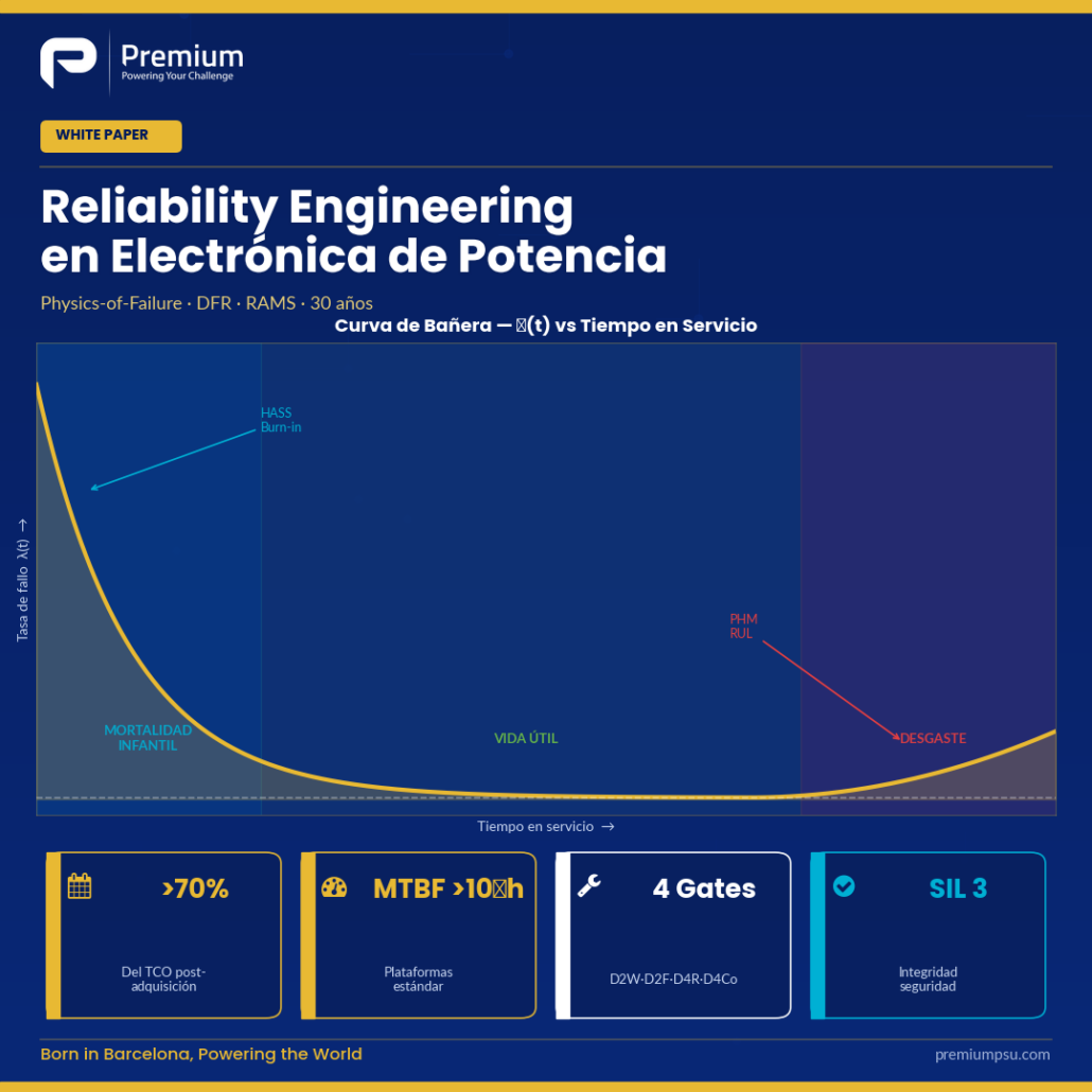
2. The Bathtub Curve — Each Phase Calls for a Different Technique

Electronic components exhibit three recognised phases: infant mortality (high initial failure rate from latent manufacturing defects), useful life (low and approximately constant rate), and wear-out (rising rate from accumulation of physical mechanisms). A mature DFR process attacks all three simultaneously.

Technique Phase Addressed When Applied Premium SA Standard
HALT (Highly Accelerated Life Testing) Design margin discovery Design phase on prototypes Combined temperature + vibration stresses beyond specification limits
HASS (Highly Accelerated Stress Screening) Latent manufacturing defects Production screening Stress levels just below operating limit; 100% of production units
Burn-in Infant mortality (left tail) Post-production, pre-delivery 4 h per unit at +60 to +80 °C; extendable to 8 h for long-interval programmes (Deutsche Bahn)

3. RAMS — The Contractual Language of Reliability

RAMS stands for Reliability, Availability, Maintainability, Safety — the four metrics with which a railway operator or grid DSO measure equipment suitability over its useful life. EN 50126 is the framework standard; EN 50128 and EN 50129 cover software and functional safety respectively.

Reliability

R(t) — probability of surviving to time t. Expressed as MTBF = 1/λ for exponential distribution, or by Weibull parameters (β, η) for wear-out phases. Premium SA calculates MTBF by PoF, not by parts-count (MIL-HDBK-217F).

Availability

A = MTBF / (MTBF + MTTR). For a substation converter with MTBF = 500,000 h and MTTR = 4 h: A ≈ 99.9992%. The key lever is not only increasing MTBF but also reducing MTTR.

Maintainability

Design levers: LRU architecture (front access, two captive screws, keyed connectors), built-in telemetry and self-test, RUL (Remaining Useful Life) estimation via PHM, and 40-year spares continuity with quarterly obsolescence review.

Safety — EN 50128 / 50129

SIL (Safety Integrity Level) per IEC 61508. PFD (Probability of Failure on Demand) for standby safety functions. SIL 3–4 requires: redundancy, periodic self-test, MC/DC software coverage metrics, formal methods. Premium SA D4Co-SW methodology aligned with EN 50128.

4. The Premium SA DFR Process — Four Sequential Gates

The Design for Reliability (DFR) methodology — originated at the Center of Reliable Power Electronics (CORPE, Aalborg University) and adopted as an internal standard at Premium SA — structures development in four sequential gates with quantitative exit criteria:

Gate Objective Key Activities Exit Criterion
D2W (Design to Work) Functional specification Mission profile definition, requirements capture, architecture selection Signed mission profile + functional test pass
D2F (Design to Function) Derating and PoF analysis Tj_max ≤ 80%, Vop ≤ 80%, thermal simulation, stress analysis All derating targets met; no RPN > 80 open
D4R (Design for Reliability) FMEA, FTA, HALT FMEA bottom-up + FTA top-down; HALT protocol; Coffin-Manson solder analysis RPN > 100 blocked; HALT limits documented; MTBF target verified
D4Co (Design for Compliance) Qualification and FRACAS HASS production screening; burn-in; EMC pre-compliance; EN 50155/EN 61373 qualification All certifications obtained; FRACAS activated; customer RAMS deliverables signed

5. FMEA, FTA and the Analytical Hierarchy

Once derating is established, reliability engineering identifies and mitigates dominant failure modes through three complementary analyses:

  • FMEA/FMECA (Failure Mode and Effects Analysis): Bottom-up. RPN = Severity × Occurrence × Detection (1–10 scale). At Premium SA, any RPN >80 triggers a documented action plan; RPN >100 blocks the D4Co gate.
  • FTA (Fault Tree Analysis): Top-down. Decomposes boolean combinations (AND/OR gates) that may cause system fault. Quantifies impact of redundancies; allows calculation of system-level MTBF.
  • ETA (Event Tree Analysis): Inductive. Models scenarios and responses derived from a single initiating event. Useful for evaluating fault propagation in multi-state systems.

6. Keeping Reliability in Service — PHM, FRACAS and Lean Reliability

PHM — Prognostics and Health Management

The active technical frontier today is the transition from fixed-schedule preventive maintenance towards maintenance based on actual condition. In Premium SA converters:

  • Real-time Tj estimation of semiconductors from Vce_sat and current, with case-temperature compensation
  • Cumulative power-cycle counting with associated ΔTj, to predict RUL (Remaining Useful Life) by PoF models
  • ESR monitoring of capacitors by ripple analysis
  • Periodic export of operating data over communication bus to the operator’s supervisor, with P-F (potential-functional) profile

FRACAS — The Continuous-Learning Loop

Failure Reporting, Analysis and Corrective Action System: every field return is analysed at the appropriate level — LRU, board, component — root cause is identified, and the corrective action is propagated to design and production. The consequence is that the population of installed equipment improves over time rather than degrading. The problem detected in unit #150 is prevented in unit #151.

About Premium SA — Premium SA is a Barcelona-based manufacturer of power electronics converters for railway, industrial and energy applications. Founded in 1981, with more than 900 standard product designs and over 40 years of operational experience, Premium SA supplies DC/DC converters, DC/AC inverters, AC/AC frequency converters, battery chargers, rectifiers and UPS systems from 50 W to 72 kW. All products are designed and manufactured at the Premium SA plant in Barcelona, with capability for EN 50155, EN 50121-3-2, EN 45545-2 and EN 61373 certification. Premium SA serves OEMs and system integrators across Europe through direct sales and a network of specialist distributors — ELIPSE (Benelux), Elma Electronic (Switzerland), RELEC Electronics (United Kingdom), DACPOL (Poland and Central Europe) and ANDA-OLSEN (Scandinavia).

Premium SA  ·  Barcelona, Spain  ·  info@premiumpsu.com  ·  +34 932 232 685  ·  www.premiumpsu.com
© 2026 Premium SA · All rights reserved · Barcelona, Spain
Born in Barcelona, Powering the World
white paper
Whitepapers

White paper – From geometry to the watt

Technical White Paper — Power Conversion Strategy

From geometry to the watt

Huawei’s temporal scaling (Tau Law and LogicFolding) and why high-voltage power delivery, close to the chip, becomes the new frontier of performance, efficiency and infrastructure cost.
Premium PSU
|
PRM-WP-2026-014
|
v1.0 · Technical draft
|
R&D · Energy · Data Center · e-Mobility
|
Internal / Partners under NDA

+53.5%
transistor density (up to 238 M/mm²)
+40%
energy efficiency in main cores
+12.7%
maximum clock frequency (up to 3.1 GHz)
1.4nm
equivalent density it aims to reach by 2031


0 — Executive summary
The constraint that shifts the frontier toward power

At ISCAS 2026 in Shanghai, Huawei proposed replacing the geometric scaling of Moore’s Law with temporal scaling: optimizing the time a signal takes to propagate through the chip (the τ constant) instead of transistor size. Its LogicFolding architecture aims to gain density and performance through 3D integration and shorter critical paths, on mature nodes that China can actually manufacture.

For Premium, what matters is not the dispute over whether τ deserves to be called a “law”. It is the inevitable physical consequence of any path that stacks more logic into less volume — whether from Huawei, TSMC, Apple or NVIDIA: power density rises, heat concentrates, and the performance ceiling is no longer set by the transistor but by the ability to deliver clean energy to the die and extract the resulting heat.

When scaling is measured in time rather than size, the bottleneck moves from the lithographer to the power engineer. High-voltage energy delivery, with conversion as close to the load as possible, goes from being infrastructure to being a lever for performance and cost.

This document traces that causal chain across four derivatives — energy consumption, performance, heat extraction and voltage architecture — and places Premium’s opportunity at the center of the last three.

1 — The paradigm shift
What Huawei proposed, and what is real about it

On May 25, 2026, He Tingbo — president of Huawei’s semiconductor business — presented the Tau (τ) Scaling Law and two supporting technologies: LogicFolding, which folds 2D circuits into vertical 3D stacks to shorten critical-path wiring, and UnifiedBus, a protocol to reduce communication latency at system level.

The core idea is sound and not new in itself: below ~10 nm, interconnect delay (the RC constant of the wiring) dominates over gate delay. The entire industry is already moving toward system scaling — backside power delivery, 3D stacking, hybrid bonding, the CFET roadmap. What Huawei does is turn that axis into corporate doctrine, because sanctions (no EUV lithography from ASML since 2023) close off the geometric axis.

Critical reading: “1.4 nm-equivalent density” is not being at 1.4 nm. It is functional density through stacking, and stacking shifts the problem — it does not eliminate it — toward three fronts that are precisely the domain of power electronics and thermal engineering:

  • Volumetric power density: more active logic in fewer mm³.
  • Current delivery: feeding the inner layers of a 3D stack without the power distribution network (PDN) “choking” them.
  • Heat dissipation: extracting heat from the interior of a solid, not just from a surface.

In other words: Huawei’s path, just like its rivals’, increases the strategic value of advanced power conversion and cooling. The rest of this document explains why.

2 — Derivative I · Energy consumption
Two layers of energy: the one that computes and the one lost along the way

The energy consumption of a computing system splits into two layers with very different dynamics:

Compute layer (on the die)

Dynamic energy follows approximately P ≈ α·C·V²·f. Reducing τ and wiring length lowers the effective capacitance C and allows, for the same frequency, operation at a lower voltage V — and the dependence on V is quadratic. This is where LogicFolding’s claimed +40% efficiency lives. It is a real gain, but confined to the chip.

Distribution and cooling layer (off the die)

At rack and data-center scale, a growing fraction of the energy never gets to compute: it is lost in voltage conversions, in distribution (I²R losses) and in moving heat (cooling overhead, reflected in PUE). As AI accelerators scale from hundreds of watts to several kilowatts per package, this second layer dominates total cost of ownership.

The efficiency the circuit designer gains inside the die can be lost — multiplied — in the power and cooling chain if the voltage architecture does not evolve at the same pace. That is Premium’s space.

3 — Derivative II · Performance
The performance ceiling is, increasingly, a power ceiling

Temporal scaling explicitly acknowledges that modern performance — and AI performance in particular — is limited by data movement, not transistor count. UnifiedBus and LogicFolding attack that “memory wall”. But there is a second wall, physical and less discussed:

  • A chip can only switch as fast as it can be fed. Increasingly aggressive current transients (di/dt) demand a very-low-impedance PDN and point-of-load (PoL) regulators millimeters from the silicon.
  • A chip can only sustain its frequency as long as it can be cooled. Thermal throttling is the most direct way a cooling shortfall turns into lost performance.

Thus, the +12.7% frequency that LogicFolding promises only materializes in the field if power delivery and thermals keep up. Delivered performance is the minimum between what the silicon can do and what the power infrastructure allows it to do.

4 — Derivative III · Heat extraction
From a surface problem to a volume problem

3D stacking changes the nature of the thermal problem. A planar chip dissipates power per unit of surface (W/cm²); a 3D stack concentrates it per unit of volume (W/cm³), and the inner layers sit far from any heat-exchange surface. The progression of solutions is well known:

Thermal stage Indicative capacity Power implication
Forced air up to ~0.5–1 kW/package Sufficient for classic SoCs; exhausted for AI.
Direct-to-chip liquid (D2C) ~1–3 kW/package Emerging standard in AI racks.
Immersion / advanced cold plate several kW Rack density >100 kW.
Embedded microfluidics (in-stack) experimental Cooling the inner layers of the 3D stack.
Critical coupling: copper versus coolant. In a 3D stack, the power delivery network (copper, vias, planes) and the cooling channels compete for the same Z-height budget. They cannot be designed separately: every watt saved in distribution losses is one less watt to extract, and every millimeter freed by a denser power architecture is space for cooling. Power and thermals become a single co-design problem.

5 — Derivative IV · Voltage architecture
Bringing high voltage close to the chip: the quadratic lever

Here lies the core of Premium’s argument. Delivered power is P = V · I. For a given power, raising the voltage V proportionally reduces the current I. And since conduction loss is Ploss = I² · R, that loss falls with the square of the current reduction. It is the difference between a linear improvement and a quadratic one.

Relative conduction loss (same power, same conductor)

high~0

100%

6.25%

0.09%

0.02%

12 V
48 V
400 V (HVDC)
800 V (HVDC)
For the same power carried by the same conductor, moving from 12 V to 48 V cuts conduction loss ~16×; stepping up to HVDC classes makes it practically negligible. The penalty then shifts to the conversion stages, which is where high-density power electronics competes.

The delivery chain and the industry’s direction

The design consequence is twofold: raise the distribution voltage and bring the final conversion closer to the load, minimizing the high-current run. The industry is already on this path:

Power delivery spine: voltage steps down and current steps up toward the die

Grid

HVDC ~400–800 V

↑ current

Rack

48 V

↑↑

Board

12 V → core

↑↑↑

PoL

<1 V

hundreds of A

Die

Goal: keep high voltage for as long a run as possible and convert to low voltage / high current only in the last millimeter.

  • Rack/row level → HVDC. The industry is migrating to DC distribution in the 400–800 V class to feed AI racks from hundreds of kW to megawatts, reducing copper, losses and the number of conversions.
  • Bus level → 48 V. The de facto standard of the modern data center (including the 48 V busbar of OCP’s Open Rack) versus legacy 12 V: same power, 1/4 of the current, ~1/16 of the loss.
  • Package level → PoL and vertical delivery. Final conversion from 48 V to core voltage (<1 V) integrated under or next to the die, and even backside power delivery, so that the very high current travels minimal distances.

Wide-bandgap (GaN and SiC) is the enabler: it allows faster, denser and more efficient converters that make this near-load conversion viable. It is exactly the terrain where Premium adds value.

6 — Infrastructure and cost
Why voltage is also a capex and opex decision

Raising the distribution voltage does not just save energy: it makes the infrastructure cheaper. The chain of effects is direct:

Lever Effect on consumption (opex) Effect on infrastructure (capex)
↑ Distribution voltage I²R loss falls with the square of the current. Thinner, cheaper conductors and busbars; less copper.
↓ Conversion stages Every conversion avoided removes its loss. Fewer conversion units, less space, fewer points of failure.
Conversion close to the load The high-current run is shortened to the minimum. Simpler PDN on the board; better use of the rack.
Fewer losses → less heat Cooling overhead drops (better PUE). Lower installed cooling capacity per useful kW.

The result is a virtuous circle: fewer losses mean less heat, which means less cooling, which means less energy and less infrastructure for the same useful power delivered to the silicon. In the era of temporal scaling — where silicon densifies without getting cheaper per node — system-level savings shift decisively to the power architecture.

7 — Premium’s positioning
Where Premium fits in this scenario

Huawei’s move illustrates a truth that applies to the whole industry, not just China: as performance densifies in volume, the advantage shifts to whoever can power and cool that volume. Premium operates precisely in that layer, and with criteria — minimum cost, open hardware/software, no vendor lock-in, performance — that fit a market looking for alternatives to both technical and geopolitical lock-in.

Lines of opportunity:

  • High-voltage to point-of-load conversion with wide-bandgap (GaN/SiC) for data center and AI: rack HVDC → 48 V → core, with the final conversion as close as possible to the die.
  • Power architectures for high-density racks aligned with OCP (48 V busbar, evolution toward HVDC), leveraging the open-hardware mandate against closed solutions.
  • Power–thermal co-design: modules where energy delivery and heat extraction are designed together, not separately — the true technical differentiator of the 3D era.
  • Vendor independence at system scale: a neutral power and thermal layer works equally under Western silicon (TSMC/Apple/NVIDIA) or the Chinese path (Huawei/Ascend), covering the ecosystem’s bifurcation.

The useful paradox: sanctions pushed Huawei down a path that increases the world’s dependence on good power delivery and cooling. That demand is agnostic as to who makes the chip — and that is precisely the neutral, open space where Premium can compete.

8 — Conclusion
The lithographer hands the baton to the power engineer

The Tau Law is neither a new law of physics nor the end of Moore; it is constraint-driven innovation. But its value for Premium is independent of whether it succeeds as a standard: any path that stacks more compute into less volume — from East or West — concentrates power and heat, and moves the performance and cost limit to the energy delivery and heat dissipation layer.

Keeping high voltage for as long a run as possible, converting close to the load with wide-bandgap technology, and co-designing power and thermals as a single problem is engineering’s answer to the era of temporal scaling. The verdict on Huawei will come with the Kirin teardowns this autumn; Premium’s is decided by how it capitalizes on a frontier that is shifting, unmistakably, into its domain.

§ Sources

  1. Huawei, official press release: “HUAWEI Presents the Tau (τ) Scaling Law” (ISCAS 2026, Shanghai, May 25, 2026).
  2. CGTN: “From geometry to time: Decoding Huawei’s Tau (τ) Scaling Law” and note on the 1.4 nm-equivalent density target for 2031.
  3. 36Kr (analysis): balanced assessment of the Tau Law and the redefinition of “mature process” as “high-performance process”.
  4. TechWire Asia: Ascend / DeepSeek V4 context and demand for domestic AI silicon.
  5. Canal TI: “Huawei busca reescribir las reglas de los procesadores” (June 8, 2026) — source article.
  6. Power engineering fundamentals (P = V·I; I²R loss; P ≈ α·C·V²·f) and distribution architecture trends (OCP Open Rack 48 V; industry migration to 400–800 V-class HVDC) — domain technical knowledge.

The LogicFolding figures (+53.5% density, +40% efficiency, +12.7% frequency, 1.4 nm-equivalent target by 2031) are Huawei’s claims pending independent validation. The voltage-loss illustrations are normalized calculations for explanatory purposes, not product specifications.


Premium PSU
PREMIUM S.A. · Power conversion systems · Barcelona
Technical White Paper PRM-WP-2026-014 · v1.0 · June 2026
Strategic analysis document. premiumpsu.com

Born in Barcelona, Powering the World

White paper – Wide bandgap semiconductors for next-generation data centers
Whitepapers

White paper – Wide bandgap semiconductors for next-generation data centers

The rapid growth of artificial intelligence, cloud computing and large-scale data processing is reshaping the energy requirements of modern data centers. In this new scenario, efficiency, power density and reliable operation under increasingly demanding loads have become key factors in power infrastructure design.

Read more
Whitepaper WTP
Whitepapers

Whitepaper WTP

Explore the latest in Wireless Power Transmission (WPT) technology for consumer electronics, healthcare, and electric vehicles. Download our expert guide to learn about high-power inductive coupling, advanced methods, and key applications in WPT. Ideal for specialists seeking detailed insights.

Read more
Maintain maximum efficiency and safety of your electronic systems in defense without compromising your equipment
Application Notes, Whitepapers

Maintain maximum efficiency and safety of your electronic systems in defense without compromising your equipment

Installing high-power electronic products in sealed enclosures presents unique challenges in terms of thermal management. This article discusses how premium power conversion products, such as the TDS-3300 and TDX-3300, can be mounted in sealed enclosures using an optimized approach for heat dissipation. The importance of sealed enclosures is highlighted, along with the use of heat sinks and thermal pads, and precise methods for calculating heat sink size and thermal resistance.


In industrial applications, sealed enclosures are essential to protect electronic systems from environmental factors such as moisture, dust, and contaminants. However, these enclosures also pose a significant challenge: effective heat dissipation. High-power conversion products like the TDS-3300, TDX-3300, ODS-3000, and ODX-3000 generate substantial amounts of heat, which, if not properly managed, can compromise performance and reduce the product’s lifespan.


Maintain maximum efficiency and safety of your electronic systems in defense without compromising your equipment

This article focuses on how to efficiently manage heat in sealed enclosures using heat sinks and thermal pads. Proper thermal planning is key to ensuring that the equipment operates within a safe temperature range without sacrificing the integrity of the sealed enclosure.

Importance of Sealed Enclosures

Sealed enclosures not only protect electronic components from external elements but also allow their use in harsh environments such as factories, outdoor settings, or marine applications. However, this isolation creates a challenge: heat buildup in a confined space. Without adequate airflow, products like the TDS-3300 and TDX-3300, originally designed to be cooled by internal fans, can overheat.

Thermal management within these enclosures is critical to avoid system failures. A well-designed enclosure, along with the installation of heat sinks, ensures that the generated heat is efficiently evacuated without compromising the enclosure’s seal.

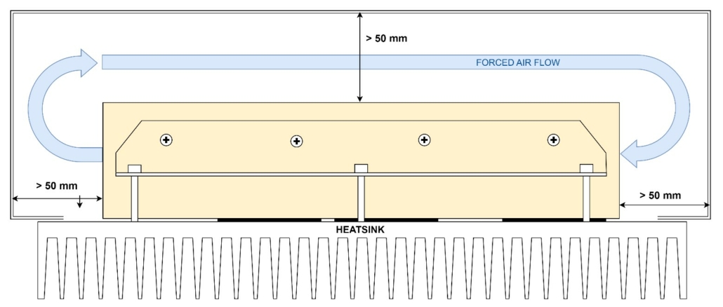
Enclosure Dimensions and Design

It is crucial that the sealed enclosure is large enough to allow proper air circulation around the device. It has been determined that a minimum space of 50 mm on each side of the product allows hot air to disperse evenly, minimizing heat buildup in critical areas.

The design of sealed enclosures must consider not only protection from external agents but also how to manage the heat generated internally. This is where heat sinks play a key role, channeling heat outside the enclosure while maintaining its airtight integrity.

Thermal Coupling with the Heat Sink

One of the most critical factors in thermal management is proper coupling between the heat sink and the product. To ensure efficient heat transfer, it is recommended to use 1 mm thick thermal pads placed strategically on the hottest surfaces of the device. These pads allow the heat sink to conduct heat out of the enclosure without requiring active airflow inside, maintaining the sealed enclosure.

Positioning of Thermal Pads

For products like the TDS-3300 or TDX-3300, thermal pads, such as the Bergquist GPVOUS-0.04-01 or equivalents, approximately 100 x 100 x 1 mm, should be placed where the internal heat sinks are closest to the outer casing. This coupling ensures efficient heat conduction from the inside to the outside of the system, where the heat sink can dissipate the heat.


Whitepaper: Multilevel converters based on GaN semiconductors
Whitepapers

Whitepaper: Multilevel converters based on GaN semiconductors

Embark on a journey into the future of power supply technology with Premium PSU’s cutting-edge whitepaper. Gain profound insights into the world of wide band-gap semiconductors and their revolutionary impact on power conversion systems.

Read more
Inverter TIPS: Soft-Start and V/f technique
Whitepapers

Inverter TIPS: Soft-Start and V/f technique

Our RDI team continously works to improve the design and functionality of our devices, so testing processes are part of day-to-day activities. Download and read this new technical article, where we offer you tips to use and maintain 3ph DC/AC inverters and methods to control induction motors.

Read more

GaN technology
Whitepapers

Introducing GaN technology in Premium PSU

Designing increasingly perfect energy solutions is our priority. Gallium nitride or GaN technology allows operation at much higher voltages, frequencies and temperatures than conventional silicon. This allows achieving increasingly compact and powerful systems. Read more

Sic-Mosfets
Whitepapers

How using SiC MOSFETs allow us to create State-of-the-Art power solutions

In our new #PremiumTech series today we show you the advantages of using SiC MOSFETs in power design, what challenges it entails and how it is crucial if we seek to maximize efficiency. SiC technology allows us to achieve very high levels of power density and performance, in a stable and compact way. Read more

A new whitepaper provides a comprehensive overview of electromagnetic interferences (EMI)
Whitepapers

A comprehensive overview of ElectroMagnetic Interferences

In our latest whitepaper, we provide a comprehensive overview of the elements that cause electromagnetic interference (EMI) and details which are the most innovative technical solutions to reduce emissions.

Read more

Page 1 of 212

Categories

  • Application Notes
  • Behind Premium PSU
  • Case Studies by industry
  • Case Studies by product
  • Custom solutions
  • Data Center
  • DC/AC inverters
  • DC/DC converters
  • Defense
  • Energy
  • Events and corporate news
  • High Tech
  • Railway & Transportation
  • Sin categoría
  • UPS
  • Whitepapers

Categoria

Premium

At Premium PSU, we are specialists in designing and manufacturing power conversion systems for the industrial market. Our product range includes high reliability power supplies from 50W to 72kW.

PREMIUM PSU
C/ Dolors Aleu, 19-21, 2nd Floor
08908 – Hospitalet de Llobregat
Barcelona-SPAIN
t.+34 93 223 26 85

Born in Barcelona Powering the World

© Copyright 2026 - Premium PSU | Power supplies equipment and systems
  • Legal Note
  • Cookie Policy
  • Complaints
  • Sales General Terms
Scroll to top Scroll to top Scroll to top
Manage Cookie Consent
We use technologies like cookies to store and/or access device information. We do this to improve browsing experience and to show (non-) personalized ads. Consenting to these technologies will allow us to process data such as browsing behavior or unique IDs on this site. Not consenting or withdrawing consent, may adversely affect certain features and functions.
Functional Always active
The technical storage or access is strictly necessary for the legitimate purpose of enabling the use of a specific service explicitly requested by the subscriber or user, or for the sole purpose of carrying out the transmission of a communication over an electronic communications network.
Preferences
The technical storage or access is necessary for the legitimate purpose of storing preferences that are not requested by the subscriber or user.
Statistics
The technical storage or access that is used exclusively for statistical purposes. The technical storage or access that is used exclusively for anonymous statistical purposes. Without a subpoena, voluntary compliance on the part of your Internet Service Provider, or additional records from a third party, information stored or retrieved for this purpose alone cannot usually be used to identify you.
Marketing
The technical storage or access is required to create user profiles to send advertising, or to track the user on a website or across several websites for similar marketing purposes.
  • Manage options
  • Manage services
  • Manage {vendor_count} vendors
  • Read more about these purposes
Preferences
  • {title}
  • {title}
  • {title}