GaN and SiC technology for power conversion systems
Gallium Nitride (GaN) and Silicon Carbide (SiC) are wide-bandgap semiconductor materials that have garnered substantial attention in the field of power electronics due to their exceptional characteristics. These materials offer several advantages over conventional silicon-based semiconductors, making them pivotal in enhancing the efficiency and performance of electronic devices, particularly in the domain of DC/DC converters and DC/AC inverters.
Gallium Nitride (GaN):
- Properties: GaN is a wide-band gap semiconductor with superior electron mobility and a higher breakdown voltage compared to silicon, affording it the capability to operate under elevated temperatures, voltages, and frequencies.
- Advantages:
- Enhanced Efficiency: GaN devices exhibit reduced on-resistance and switching losses, resulting in superior efficiency during power conversion.
- Compact Form Factor: GaN-based devices enable compact designs due to their higher power density, rendering them suitable for miniaturization.
- Rapid Switching: GaN transistors can achieve faster switching transitions compared to silicon, thereby diminishing switching losses.
- Applications:
- DC/DC Converters: GaN devices are employed to enhance the efficiency of voltage converters such as buck and boost converters, specifically in applications such as electric vehicles and data centers.
- DC/AC Inverters: GaN-based inverters find utility in renewable energy systems, such as solar inverters, and motor drives, thus elevating energy conversion efficiency and control.
Silicon Carbide (SiC):
- Properties: SiC is another wide-band gap semiconductor renowned for its high-temperature stability and superior electrical characteristics. It is capable of handling higher voltages and temperatures than silicon.
- Advantages:
- High Voltage Operation: SiC devices are operable at elevated voltage levels, obviating the need for intricate voltage stacking configurations in power systems.
- Reduced Conduction Losses: SiC’s lower on-resistance translates to diminished conduction losses and improved efficiency.
- Thermal Endurance: SiC can endure extreme temperatures, rendering it suitable for deployment in demanding environments.
- Applications:
- DC/DC Converters: SiC components play a pivotal role in power converters tailored for high-voltage applications, such as electric vehicles and renewable energy systems.
- DC/AC Inverters: SiC inverters are of paramount importance in transforming DC power from sources like batteries into AC power for grid integration or motor drives in railway applications, thereby achieving higher efficiency and power density.
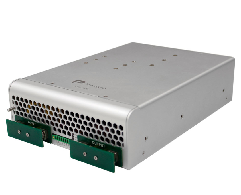
- CRS-2000 DC/DC Converter
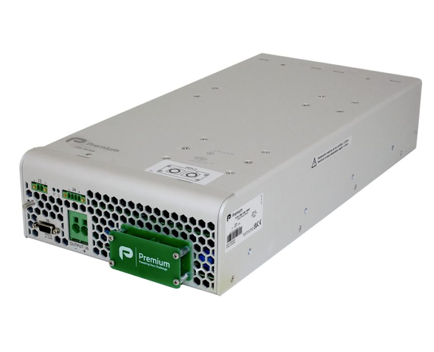
- CBS-10K DC/DC Converter
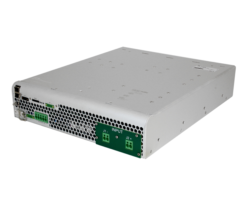
- OVX-6400 DC/AC Inverter
- FlexStorm AC/DC High Frequency Rectifier
Significance in Enhancing Efficiency and Performance:
Both GaN and SiC power semiconductor technologies substantially enhance the efficiency and performance of electronic devices, particularly in DC/DC converters and DC/AC inverters, through the following means:
- Loss Reduction: GaN and SiC devices manifest reduced conduction and switching losses, culminating in enhanced efficiency and heat dissipation.
- Elevated Power Density: Their compact dimensions and improved thermal characteristics facilitate greater power density, leading to the design of smaller and lighter power electronic systems.
- Extended Operational Range: GaN and SiC can operate under higher temperature and voltage conditions, augmenting the reliability and durability of electronic devices.
- Enhanced Switching Dynamics: The rapid switching capabilities of these materials enable more precise control, mitigating distortion and elevating overall system performance.
Advantages of GaN and SiC Devices
Exploring deeper into how the advantages of Gallium Nitride (GaN) and Silicon Carbide (SiC) semiconductors, translate into improved performance in DC/DC converters and DC/AC inverters, particularly in terms of higher efficiency and power density.
Improved Efficiency:
- Reduced Switching Losses: GaN and SiC semiconductors have a distinct advantage of faster switching speeds compared to traditional silicon. This rapid switching capability significantly reduces switching losses in DC/DC converters and DC/AC inverters. As a result, a smaller portion of the input power is dissipated as heat during each switching cycle, leading to higher overall efficiency.
- Lower Conduction Losses: Both GaN and SiC exhibit lower on-resistance when compared to silicon, which means they have less resistance to the flow of current. In DC/DC converters and DC/AC inverters, this translates to reduced conduction losses as the devices handle high currents. Lower conduction losses mean a higher proportion of the input power is effectively delivered to the load, contributing to improved efficiency.
- High-Temperature Tolerance: GaN and SiC can operate at elevated temperatures without significant degradation in performance. In DC/DC converters and DC/AC inverters, where heat generation is a concern, the ability to function at higher temperatures allows for efficient operation without the need for excessive cooling, further enhancing overall efficiency.
Increased Power Density:
- Compact Size: GaN and SiC devices are known for their superior power density, meaning they can handle higher power levels in a smaller physical footprint. In DC/DC converters and DC/AC inverters, this compact size allows for more efficient use of space, which is especially crucial in applications with limited installation space or where minimizing weight is essential, such as in electric vehicles.
- Higher Voltage Handling: SiC can handle higher voltage levels than silicon, which simplifies the design of high-voltage DC/DC converters and DC/AC inverters. Fewer components are required to achieve the desired voltage levels, leading to a more compact and power-dense system.
- Reduced Cooling Requirements: The improved efficiency and thermal characteristics of GaN and SiC devices reduce the need for elaborate cooling systems. In DC/DC converters and DC/AC inverters, this not only saves space but also allows for the design of more compact and lightweight systems.
The advantages of GaN and SiC semiconductors, including reduced switching and conduction losses, high-temperature tolerance, compact size, and higher voltage handling, directly translate into improved performance in power conversion systems.
These improvements result in higher efficiency, meaning a larger proportion of input power is converted into useful output power, and greater power density, enabling the development of smaller, more powerful, and energy-efficient electronic systems. These benefits are particularly significant in applications such as electric vehicles, renewable energy systems, industrial automation and, railway industry, where space, weight, and energy efficiency are critical considerations.
Challenges and Future Developments
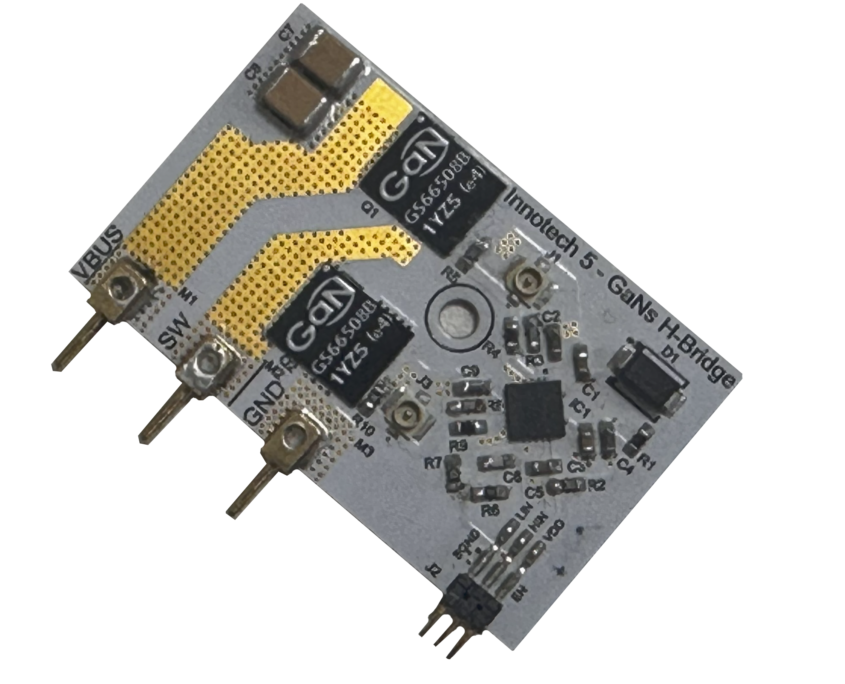
Premium PSU is incorporating Gallium Nitride (GaN) technology into their devices thorough the collaboration with the ALL2GaN project. GaN technology is known for its potential to significantly improve the performance of electronic devices in various applications. The project is focused on evaluating and quantifying the benefits of these new GaN devices in real-world RF and power applications, particularly in railway applications.
Some key aspects of the project:
- Collaboration with ALL2GaN: We are partnering with the ALL2GaN project, which aims to conduct industrial research on affordable and environmentally friendly GaN technologies. This collaboration suggests a commitment to advancing GaN technology for a wide range of applications.
- Research and Development (R&D): Our RDI department is actively involved in updating existing equipment to incorporate GaN technology. This R&D work is crucial for integrating GaN into your devices effectively.
- Application Fields: ALL2GaN work plan focuses on three main application fields:
- Radio Frequency and Communication: GaN technology can significantly enhance the efficiency and performance of RF and communication systems, such as in the development of high-frequency and high-power amplifiers.
- Electric Mobility: GaN can be used to improve the efficiency and performance of electric mobility solutions, including railways and electric vehicles. This can contribute to the reduction of carbon emissions and a more sustainable transportation system.
- Energy: GaN technology can benefit various energy-related applications, including photovoltaics (PV), DC microgrids, and lighting. These applications can help address climate and energy challenges.
- Objectives: Our objectives include assessing and demonstrating the higher efficiencies, higher switching frequencies, and higher power densities of GaN applications without compromising reliability. Achieving these objectives can lead to more efficient and environmentally friendly electronic systems.
- Prototypes: We plan to develop prototypes in Work Plan 6 (WP6) to showcase the potential of the GaN devices in improving system performance. This could have a significant impact on achieving the overall goals of the project and contributing to “objective 7.”
- Environmental and Social Impact: This project wants to be conscious of the broader impact of GaN technology on addressing climate and social challenges. GaN technology, by increasing efficiency and reducing energy consumption, can have a positive environmental impact. Additionally, improving electric mobility and energy applications aligns with sustainability objectives.

